Breakover Current IBO Max
:
Rated Repetitive Off-State Voltage VDRM
:
Off-State Leakage Current @ VDRM IDRM
:
On-State RMS Current (It RMS)
:
Forward Voltage Drop
:
Gate Trigger Voltage (Vgt)
:
Maximum Gate Peak Inverse Voltage
:
Gate Trigger Current (Igt)
:
Holding Current (Ih Max)
:
Packaging
:
Mounting Style
: SMD/SMT
Package / Case
: SOIC-8
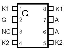
Pinout Specifications
|
RATING |
SYMBOL |
VALUE |
UNIT |
| Repetitive peak off-state voltage, IG = 0 |
VDRM |
-100 |
V |
| Repetitive peak gate-cathode voltage, VKA = 0 |
VGKRM |
-99 |
V |
Non-repetitive peak on-state pulse current (see Notes 1 and 2)
10/1000 µs (Bellcore GR-1089-CORE, Issue 2, December 1997, Section 4)
0.2/310 µs (I3124, open-circuit voltage wave shape 0.5/700 µs)
5/310 µs (ITU-T K20 & K21, open-circuit voltage wave shape 10/700 µs)
1/20 µs (ITU-T K22, open-circuit voltage wave shape 1.2/50 µs)
2/10 µs (Bellcore GR-1089-CORE, Issue 2, December 1997, Section 4) |
ITSP |
30
40
40
100
100
|
A |
Non-repetitive peak on-state current, 50/60 Hz (see Notes 1 and 2)
100 ms
1 s
5 s
300 s
900 s
|
ITSM |
11
4.5
2.4
0.95
0.93 |
A |
| Non-repetitive peak gate current, 1/2 µs pulse, cathodes commoned (see Note 1) |
IGSM |
40 |
A |
| Operating free-air temperature range |
TA |
-40 to +85 |
°C |
| Junction temperature |
TJ |
-40 to +150 |
°C |
| Storage temperature range |
Tstg |
-65 to +150 |
°C |
DescriptionThe TISPPBL1 and TISPPBL2 are dual forward-conducting buffered p-gate overvoltage protectors. They are designed to protect the Ericsson Components SLICs (Subscriber Line Interface Circuits) against overvoltages on the telephone line caused by lightning, a.c. power contact and induction. The TISPPBLx limits voltages that exceed the SLIC supply rail levels.
The SLIC line driver section TISPPBL1 and TISPPBL2 is typically powered by a negative voltage, VBat, in the region of -10 V to -85 V. The protector gate is connected to this negative supply. This references the protection (clipping) voltage to the negative supply voltage. As the protection voltage will track the negative supply voltage the overvoltage stress on the SLIC is minimised. The TISPPBLx buffered gate design reduces the loading on the SLIC supply during overvoltages caused by power cross and induction.
Positive overvoltages TISPPBL1 and TISPPBL2 are clipped to ground by diode forward conduction. Negative overvoltages are initially clipped close to the SLIC negative supply rail value. If sufficient current is available from the overvoltage, then the protector will crowbar into a low voltage ground referenced on-state condition. As the overvoltage subsides the high holding current of the crowbar prevents d.c. latchup. The difference between the TISPPBL1 and TISPPBL2 is the minimum value of holding current. The 105 mA TISPPBL1 can delatch SLIC programmed line currents up to 55 mA and the 150 mA TISPPBL2 can delatch all programmed line current values.
These monolithic protection devices TISPPBL1 and TISPPBL2 are fabricated in ion-implanted planar vertical power structures for high reliability and in normal system operation they are virtually transparent. The TISPPBLx is available in 8-pin plastic small-outline surface mount package and 8-pin plastic dual-in-line package.

 TISPPBL1D Data Sheet


