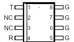
PinoutSpecifications RATING SYMBOL VALUE UNIT Repetitive peak off-state voltage R-G terminals T-G terminals VDRM -180, +105-105, +105 v Non-repetitive peak on-state pulse current (see Notes 1, 2 and 3) 2/10 µs (GR-1089-CORE, 2/10 µs voltage wave shape) 8/20 &...
TISPL758LF3D: PinoutSpecifications RATING SYMBOL VALUE UNIT Repetitive peak off-state voltage R-G terminals T-G terminals VDRM -180, +105-105, +105 v Non-repetitive peak on-state pulse ...
SeekIC Buyer Protection PLUS - newly updated for 2013!
268 Transactions
All payment methods are secure and covered by SeekIC Buyer Protection PLUS.
PinoutSpecifications Rating Symbol Value Unit Repetitive peak off-state voltage...
PinoutSpecifications RATING SYMBOL VALUE UNIT Repetitive peak off-state voltage ( 0°C &...
RATING |
SYMBOL |
VALUE |
UNIT |
Repetitive peak off-state voltage R-G terminals T-G terminals |
VDRM | -180, +105 -105, +105 |
v |
Non-repetitive peak on-state pulse current (see Notes 1, 2 and 3) 2/10 µs (GR-1089-CORE, 2/10 µs voltage wave shape) 8/20 µs (ANSI C62.41, open-circuit voltage wave shape ) 10/160 µs (FCC Part 68, open-circuit voltage wave shape ) 5/200 µs (VDE 0433, open-circuit voltage wave shape ) 0.2/310 µs (I3124, 2.0 kV, 0.5/700 µs voltage wave shape) 5/310 µs (ITU-T K20/21, 2.0 kV, 10/700 µs voltage wave shape) 5/310 µs (FTZ R12, open-circuit voltage wave shape ) 10/560 µs (FCC Part 68, open-circuit voltage wave shape ) 10/1000 µs (GR-1089-CORE, 10/1000 µs voltage wave shape) |
ITSP |
175 120 60 50 50 50 50 45 35 |
A |
Non-repetitive peak on-state current (see Notes 1, 2 and 3) full sine wave 50 Hz 60 Hz |
ITSM |
16 20 |
A |
Repetitive peak on-state current, 50/60 Hz, (see Notes 2 and 3) |
ITSM |
2x1 |
A |
Initial rate of rise of on-state current, Exponential current ramp, Maximum ramp value < 70 A |
diT/dt |
150 |
A/µs |
Junction temperature |
TJ |
-40 to +150 |
°C |
Storage temperature range |
Tstg |
-40 to +150 |
°C |
The TISPL758LF3 is an integrated combination of a symmetrical bidirectional overvoltage protector and an asymmetrical bidirectional overvoltage protector. It is designed to limit the peak voltages on the line terminals of the Lucent Technologies L7581/2/3 LCAS (Line Card Access Switches). An LCAS may also be referred to as a Solid State Relay, SSR, i.e. a replacement of the conventional electromechanical
relay.
The TISPL758LF3D voltages are chosen to give adequate LCAS protection for all switch conditions. The most potentially stressful the TISPL758LF3D limits the voltage and corresponding LCAS dissipation until the LCAS thermal trip operates and opens the switches.
Under open-circuit ringing conditions, the line ring (R) conductor will have high peak voltages. For battery backed ringing, the ring conductor will have a larger peak negative voltage than positive i.e. the peak voltages are asymmetric. An overvoltage protector with a similar voltage asymmetry will give the most effective protection. On a connected line, the tip (T) conductor will have much smaller voltage levels than the opencircuit ring conductor values. Here a symmetrical voltage protector gives adequate protection.
Overvoltages are normally caused by a.c. power system or lightning flash disturbances which are induced or conducted on to the telephone line. These overvoltages are initially clipped by protector breakdown clamping until the voltage rises to the breakover level, which causes the