On-State RMS Current (It RMS)
:
Forward Voltage Drop
:
Gate Trigger Voltage (Vgt)
:
Maximum Gate Peak Inverse Voltage
:
Gate Trigger Current (Igt)
:
Holding Current (Ih Max)
:
Breakover Current IBO Max
:
Off-State Leakage Current @ VDRM IDRM
: 0.01 mA
Packaging
: Tube
Mounting Style
: SMD/SMT
Rated Repetitive Off-State Voltage VDRM
: 100 V
Package / Case
: SOIC-8
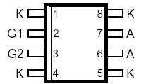
Pinout Specifications
|
RATING |
SYMBOL |
VALUE |
UNIT |
| Repetitive peak off-state voltage, 0 °C to 70 °C |
VDRM |
100 |
V |
Non-repetitive peak on-state pulse current (see Notes 1 and 2)
10/1000 µs (GR-1089-CORE, open-circuit voltage wave shape 10/1000 µs)
5/310 µs (CCITT K20/21, open-circuit voltage wave shape 7 kV10/700 µs)
8/20 µs (ANSI C62.41, open-circuit voltage wave shape 1.2/50 µs) |
ITSP |
150
150
500 |
A |
Non-repetitive peak on-state current, 50 Hz, halfwave rectified sinewave, (see Notes 1 and 2)
100 ms
1 s
900 s
|
ITSM |
22
8
3 |
A |
| Junction temperature |
TJ |
-40 to +150 |
°C |
| Storage temperature range |
Tstg |
-65 to +150 |
°C |
DescriptionThe TISP83121D is a dual-gate reverse-blocking unidirectional thyristor designed for the protection of dual-voltage ringing SLICs (Subscriber Line Interface Circuits) against overvoltages on the telephone line caused by lightning, a.c. power contact and induction.
The device chip is a four-layer NPNP silicon thyristor structure which has an electrode connection to every layer. For negative overvoltage protection the TISP83121D is used in a common anode configuration with the voltage to be limited applied to the cathode (K) terminal and the negative reference potential applied to the gate 1 (G1) terminal. For positive overvoltage protection the TISP83121D is used in a common cathode configuration with the voltage to be limited applied to the anode (A) terminal and the positive reference potential applied to the gate 2 (G2) terminal.
The TISP83121D is a unidirectional protector and to prevent reverse bias, requires the use of a series diode between the protected line conductor and the protector. Further, the gate reference supply voltage requires an appropriately poled series diode to prevent the supply from being shorted when the TISP83121D crowbars.
Under low level power cross conditions the TISP83121D gate current will charge the gate reference supply. If the reference supply cannot absorb the charging current its potential will increase, possibly to damaging levels. To avoid excessive voltage levels a clamp (zener or avalanche breakdown diode) may be added in shunt with the supply. Alternatively, a grounded collector emitter-follower may be used to reduce the charging current by the transistors HFE value.
This monolithic protection device is made with a ion-implanted epitaxial-planar technology to give a consistent protection performance and be virtually transparent to the system in normal operation.

 TISP83121D Data Sheet


