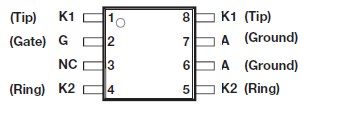
PinoutSpecifications Rating Symbol Value Unit Repetitive peak off-state voltage, VGK = 0 VDRM -170 V Repetitive peak gate-cathode voltage, VKA = 0 VGKRM -167 V Non-repetitive peak impulse current (see Notes 1, 2 and 3)10/1000 s (Telcordia GR-1089-CO...
TISP61089HDM: PinoutSpecifications Rating Symbol Value Unit Repetitive peak off-state voltage, VGK = 0 VDRM -170 V Repetitive peak gate-cathode voltage, VKA = 0 VGKRM -167...
SeekIC Buyer Protection PLUS - newly updated for 2013!
268 Transactions
All payment methods are secure and covered by SeekIC Buyer Protection PLUS.
PinoutSpecifications Rating Symbol Value Unit Repetitive peak off-state voltage...
PinoutSpecifications RATING SYMBOL VALUE UNIT Repetitive peak off-state voltage ( 0°C &...
Rating |
Symbol |
Value |
Unit |
Repetitive peak off-state voltage, VGK = 0 |
VDRM |
-170 |
V |
Repetitive peak gate-cathode voltage, VKA = 0 |
VGKRM |
-167 |
V |
Non-repetitive peak impulse current (see Notes 1, 2 and 3) 10/1000 s (Telcordia GR-1089-CORE, Issue 3) 5/310 s (ITU-T K.20, K.21 & K.45, K.44 open-circuit voltage wave shape 10/700 s) 10/360 s (Telcordia GR-1089-CORE, Issue 3) 1.2/50 s voltage waveshape (Telcordia GR-1089-CORE, Issue 3), including 3 non-inductive resistor 2/10 s (Telcordia GR-1089-CORE, Issue 3) |
IPPSM |
100 150 100 500 500 |
A |
Non-repetitive peak on-state current, 50 Hz / 60 Hz (see Notes 1, 2, 3 and 4) 0.5 s 1 s 2 s 5 s 30 s 900 s |
ITSM |
7.7 6.1 4.8 3.7 2.8 2.6 |
A |
Junction temperature |
TJ |
-40 to +150 |
°C |
Storage temperature range |
Tstg |
-65 to +150 |
°C |
NOTES: 1. Initially the device must be in thermal equilibrium with TJ = 25 °C. The surge may be repeated after the device returns to its initial conditions. 2. The rated current values may be applied either to the Ring to Ground or to the Tip to Ground terminal pairs. Additionally, both terminal pairs may have their rated current values applied simultaneously (in this case the Ground terminal current will be twice the rated current value of an individual terminal pair). Ratings are obtained by using the gate circuitry as shown in Fig. 3. 3. Rated currents only apply if pins 1 & 8 (Tip) are connected together, pins 4 & 5 (Ring) are connected together and pins 6 & 7 (Anode) are connected together. 4. EIA/JESD51-2 environment and EIA/JESD51-7 high effective thermal conductivity test board (multi-layer) connected with 0.6 mm printed wiring track widths.
The TISP61089HDM is a dual forward-conducting buffered p-gate thyristor (SCR) overvoltage protector. It is designed to protect monolithic SLICs (Subscriber Line Interface Circuits) against overvoltages on the telephone line caused by lightning, a.c. power contact and induction. The TISP61089HDM limits voltages that exceed the SLIC supply rail voltage. The TISP61089HDM parameters are specified to allow equipment compliance with Telcordia GR-1089-CORE, Issue 3 and ITU-T recommendations K.20, K.21 and K.45.
The SLIC line driver section TISP61089HDM is typically powered from 0 V (ground) and a negative voltage in the region of -20 V to -155 V. The protector gate is connected to this negative supply. This references the protection (clipping) voltage to the negative supply voltage. The protection voltage will then track the negative supply voltage and the overvoltage stress on the SLIC is minimized.