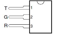
PinoutSpecifications Rating Symbol Value Unit Repetitive peak off-state voltage, (see Note 1)'3070'3080'3095'3115'3125'3135'3145'3180'3210'3250'3290'3350 VDRM ± 58± 65± 75±90±100±110±120±145±160±190±220±275 V Non-repetitive peak on-state pulse current (see Notes 2, 3...
TISP3095H3: PinoutSpecifications Rating Symbol Value Unit Repetitive peak off-state voltage, (see Note 1)'3070'3080'3095'3115'3125'3135'3145'3180'3210'3250'3290'3350 VDRM ± 58± 65± 75±9...
SeekIC Buyer Protection PLUS - newly updated for 2013!
268 Transactions
All payment methods are secure and covered by SeekIC Buyer Protection PLUS.
PinoutSpecifications Rating Symbol Value Unit Repetitive peak off-state voltage...
PinoutSpecifications RATING SYMBOL VALUE UNIT Repetitive peak off-state voltage ( 0°C &...
Rating |
Symbol |
Value |
Unit |
Repetitive peak off-state voltage, (see Note 1) '3070 '3080 '3095 '3115 '3125 '3135 '3145 '3180 '3210 '3250 '3290 '3350 |
VDRM |
|
V |
Non-repetitive peak on-state pulse current (see Notes 2, 3 and 4) 2/10 s (GR-1089-CORE, 2/10 s voltage wave shape) 8/20 s (IEC 61000-4-5, 1.2/50 s voltage, 8/20 current combination wave generator) 10/160 s (FCC Part 68, 10/160 s voltage wave shape) 5/200 s (VDE 0433, 10/700 s voltage wave shape) 0.2/310 s (I3124, 0.5/700 s voltage wave shape) 5/310 s (ITU-T K.20/21, 10/700 s voltage wave shape) 5/310 s (FTZ R12, 10/700 s voltage wave shape) 5/320 s (FCC Part 68, 9/720 s voltage wave shape) 10/560 s (FCC Part 68, 10/560 s voltage wave shape) 10/1000 s (GR-1089-CORE, 10/1000 s voltage wave shape) |
ITSP |
500 300 250 220 200 200 200 160 100 |
A |
Non-repetitive peak on-state current (see Notes 2, 3 and 5) 20 ms (50 Hz) full sine wave 16.7 ms (60 Hz) full sine wave 1000 s 50 Hz/60 Hz a.c. |
ITSM |
55 60 1 |
A |
Initial rate of rise of on-state current, Exponential current ramp, Maximum ramp value < 200 A |
diT/dt |
400 |
A/s |
Junction temperature |
TJ |
-40 to +150 |
°C |
Storage temperature range |
Tstg |
-65 to +150 |
°C |
NOTES: 1. See Figure 9 for voltage values at lower temperatures.
2. Initially the TISP3xxxH3SL must be in thermal equilibrium.
3. These non-repetitive rated currents are peak values of either polarity. The rated current values may be applied to the R or T terminals. Additionally, both R and T terminals may have their rated current values applied simultaneously (in this case the G terminal return current will be the sum of the currents applied to the R and T terminals). The surge may be repeated after the TISP3xxxH3SL returns to its initial conditions.
4. See Figure 10 for impulse current ratings at other temperatures. Above 85 °C, derate linearly to zero at 150 °C lead temperature.
5. EIA/JESD51-2 environment and EIA/JESD51-3 PCB with standard footprint dimensions connected with 5 A rated printed wiring track widths. See Figure 8 for the current ratings at other durations. Figure 8 shows the R and T terminal current rating for simultaneous operation. In this condition, the G terminal current will be 2xITSM(t), the sum of the R and T terminal currents. Derate current values at -0.61 %/°C for ambient temperatures above 25 °C.
The TISP3xxxH3SL limits overvoltages between the telephone line Ring and Tip conductors and Ground. Overvoltages are normally caused by a.c. power system or lightning flash disturbances which are induced or conducted on to the telephone line.
The protector TISP3xxxH3SL consists of two symmetrical voltage-triggered bidirectional thyristors. Overvoltages are initially clipped by breakdown clamping until the voltage rises to the breakover level, which causes the device to crowbar into a low-voltage on state. This low-voltage on state causes the current resulting from the overvoltage to be safely diverted through the device. The high crowbar holding current prevents d.c. latchup as the diverted current subsides.