THS5651A

Features: 􀀀 Member of the Pin-Compatible CommsDACTM Product Family􀀀 125 MSPS Update Rate􀀀 10-Bit Resolution􀀀 Superior Spurious Free Dynamic Range Performance (SFDR) to Nyquist at 40 MHz Output: 62 dBc􀀀 1 ns Setup/Hold Time􀀀 Differential Scalabl...

product image

THS5651A Picture
SeekIC No. : 004518912 Detail

THS5651A: Features: 􀀀 Member of the Pin-Compatible CommsDACTM Product Family􀀀 125 MSPS Update Rate􀀀 10-Bit Resolution􀀀 Superior Spurious Free Dynamic Range Performance (SFD...

floor Price/Ceiling Price

Part Number:
THS5651A
Supply Ability:
5000

Price Break

  • Qty
  • 1~5000
  • Unit Price
  • Negotiable
  • Processing time
  • 15 Days
Total Cost: $ 0.00

SeekIC Buyer Protection PLUS - newly updated for 2013!

  • Escrow Protection.
  • Guaranteed refunds.
  • Secure payments.
  • Learn more >>

Month Sales

268 Transactions

Rating

evaluate  (4.8 stars)

Upload time: 2025/1/12

Payment Methods

All payment methods are secure and covered by SeekIC Buyer Protection PLUS.

Notice: When you place an order, your payment is made to SeekIC and not to your seller. SeekIC only pays the seller after confirming you have received your order. We will also never share your payment details with your seller.
Product Details

Description


Features:

􀀀 Member of the Pin-Compatible CommsDACTM Product Family
􀀀 125 MSPS Update Rate
􀀀 10-Bit Resolution
􀀀 Superior Spurious Free Dynamic Range Performance (SFDR) to Nyquist at 40 MHz
    Output: 62 dBc
􀀀 1 ns Setup/Hold Time
􀀀 Differential Scalable Current Outputs: 2 mA to 20 mA
􀀀 On-Chip 1.2-V Reference
􀀀 3 V and 5 V CMOS-Compatible Digital Interface
􀀀 Straight Binary or Twos Complement Input
􀀀 Power Dissipation: 175 mW at 5 V, Sleep Mode: 25 mW at 5 V
􀀀 Package: 28-Pin SOIC and TSSOP


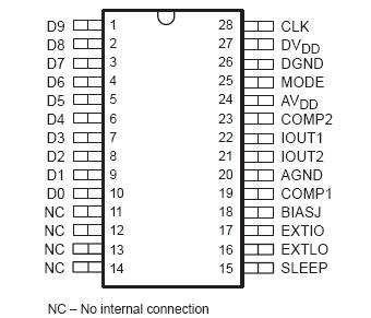
Pinout

  Connection Diagram


Specifications

Supply voltage range, AVDD  . . . . . . . . . . . . . . . . . . . . . . . . . . . . . . . . . . . . . . . . . . . . 0.3 V to 6.5 V
                                    DVDD  . . . . . . . . . . . . . . . . . . . . . . . . . . . . . . . . . . . . . . . . . . . 0.3 V to 6.5 V
Voltage between AGND and DGND . . . . . . . . . . . . . . . . . . . . . . . . . . . . . . . . . . . . . . .  0.3 V to 0.5 V
Supply voltage range, AVDD to DVDD . . . . . . . . . . . . . . . . . . . . . . . . . . . . . . . . . . . . . . 6.5 V to 6.5 V
                                   CLK, SLEEP, MODE . . . . . . . . . . . . . . . . . . . . . .. . . . . . 0.3 V to DVDD + 0.3 V
                                   Digital input D9D0  . . . . . . . . . . . . . . . . . . . . ... . . . . . . 0.3 V to DVDD + 0.3 V
                                   IOUT1, IOUT2 . . . . . . . . . . . . . . . . . . . . . . . . . .  . . . . . . . . . 1 V to AVDD + 0.3 V
                                   COMP1, COMP2  . . . . . . . . . . . . . . . . . . . . . . .  . . . . . . . 0.3 V to AVDD + 0.3 V
                                   EXTIO, BIASJ  . . . . . . . . . . . . . . . . . . . . . . .  . . . . . . . . . . 0.3 V to AVDD + 0.3 V
                                   EXTLO  . . . . . . . . . . . . . . . . . . . . . . . . . . . . . . . . . . . . . . . . . . 0.3 V to 0.3 V
Peak input current (any input) . . . . . . . . . . . . . . . . . . . . . . . . . . . . . . . . . . . . . . . . . . . . . . . . . . 20 mA
Peak total input current (all inputs) . . . . . . . . . . . . . . . . . . . . . . . . . . . . . . . . . . . . . . . . . . . . .  30 mA
Operating free-air temperature range, TA: THS5651AI . . . . . . . . . . . . . . . . . . . . . . . . . 40°C to 85°C
Storage temperature range . . . . . . . . . . . . . . . . . . . . . . . . . . . . . . . . . . . . . . . . . . . . . . 65°C to 150°C
Lead temperature 1,6 mm (1/16 inch) from the case for 10 seconds . . . . . . . . . . . . . . . . . . . . . . 260°C


Description

The THS5651A is a 10-bit resolution digital-to-analog converter (DAC) specifically optimized for digital data transmission in wired and wireless communication systems. The 10-bit DAC is a member of the CommsDAC series of high-speed, low-power CMOS digital-to-analog converters. The CommsDAC family consists of pin compatible 14-, 12-, 10-, and 8-bit DACs. All devices offer identical interface options, small outline package and pinout. The THS5651A offers superior ac and dc performance while supporting update rates up to 125 MSPS.

The THS5651A operates from an analog supply of 4.5 V to 5.5 V. Its inherent low power dissipation of 175 mW ensures that the device is well suited for portable and low-power applications. Lowering the full-scale current output reduces the power dissipation without significantly degrading performance. The device features a SLEEP mode, which reduces the standby power to approximately 25 mW, thereby optimizing the power consumption for system needs.The THS5651A is manufactured in Texas Instruments advanced high-speed mixed-signal CMOS process. A current-source-array architecture combined with simultaneous switching shows excellent dynamic performance. On-chip edge-triggered input latches and a 1.2 V temperature compensated bandgap reference provide a complete monolithic DAC solution. The digital supply range of 3 V to 5.5 V supports 3 V and 5 V CMOS logic families. Minimum data input setup and hold times allow for easy interfacing with external logic. The THS5651A supports both a straight binary and twos complement input word format, enabling flexible interfacing with digital signal processors.

The THS5651A provides a nominal full-scale differential output current of 20 mA and >300 kW output impedance, supporting both single-ended and differential applications. The output current can be directly fed to the load (e.g., external resistor load or transformer), with no additional external output buffer required. An accurate on-chip reference and control amplifier allows the user to adjust this output current from 20 mA down to 2 mA, with no significant degradation of performance. This reduces power consumption and provides 20 dB gain range control capabilities. Alternatively, an external reference voltage and control amplifier may be applied in applications using a multiplying DAC. The output voltage compliance range is 1.25 V.The THS5651A is available in both a 28-pin SOIC and TSSOP package. The THS5651A is characterized for operation over the industrial temperature range of 40°C to 85°C.


Customers Who Bought This Item Also Bought

Margin,quality,low-cost products with low minimum orders. Secure your online payments with SeekIC Buyer Protection.
Potentiometers, Variable Resistors
Audio Products
Tapes, Adhesives
803
Connectors, Interconnects
View more