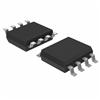
Features: ` Fully Differential Architecture` Centered Input Common-mode Range` Minimum Gain of 2V/V (6 dB)` Bandwidth: 1900 MHz (100 mVpp, G = 10 dB,RL = 200 W)` Slew Rate: 6600 V/µs (2V step, G = 10 dB)` 1% Settling Time: 2 ns (2 V step, G = 10 dB)` HD2: 75 dBc at 100 MHz (2 Vpp, G = 10 dB,...
THS4509: Features: ` Fully Differential Architecture` Centered Input Common-mode Range` Minimum Gain of 2V/V (6 dB)` Bandwidth: 1900 MHz (100 mVpp, G = 10 dB,RL = 200 W)` Slew Rate: 6600 V/µs (2V step,...
SeekIC Buyer Protection PLUS - newly updated for 2013!
268 Transactions
All payment methods are secure and covered by SeekIC Buyer Protection PLUS.
VS to VS+ VI VID IO TJ TA Tstg |
Supply voltage Input voltage Differential input voltage Output current(1) Continuous power dissipation Maximum junction temperature Operating free-air temperature range Storage temperature range Lead temperature 1,6 mm (1/16 inch) from case for 10 seconds |
UNIT 6 V ±VS 4 V 200 mA See Dissipation Rating Table 150°C 40°C to 85°C 65°C to 150°C 300°C |
The THS4509 is a wideband, fully differential op amp designed for 5 V data acquisition systems. It has very low noise at 1.9 nV/ÖHz, and extremely low harmonic distortion of 75 dBc HD2 and 80 dBc HD3 at 100 MHz with 2 Vpp, G = 10 dB, and 1 kW load. Slew rateis very high at 6600 Vµs and with settling time of 2 ns to 1% (2 V step)THS4509 is ideal for pulsed applications. It is designed for minimum gain of 6 dB, but is optimized for gain of 10 dB.
To allow for dc coupling to ADCs, THS4509's unique output common-mode control circuit maintains the output common-mode voltage within 3 mV offset (typ) from the set voltage, when set within 0.5 V of mid-supply, with less than 4 mV differential offset voltage. The common-mode set point is set to mid-supply by internal circuitry, THS4509 may be over-driven from an external source.