Features: ` Fully Differential Architecture
` Centered Input Common-mode Range
` Minimum Gain of 2V/V (6 dB)
` Bandwidth: 1900 MHz
` Slew Rate: 6600 V/µs
` 0.1% Settling Time: 2 ns
` HD2: 75 dBc at 100 MHz for gain of 10 dB.
` HD3: 80 dBc at 100 MHz
` OIP2: 73 dBm at 70 MHz
` OIP3: 37 dBm at 70 MHz
` Input Voltage Noise: 1.9 nV/ (f >10 MHz)
` Noise Figure: 17.1 dB
` Output Common-Mode Control
` Power Supply:
` Voltage: 3 V (±1.5 V) to 5 V (±2.5 V)
` Current: 37.7 mA
` Power-Down Capability: 0.65 mA
Application· 5 V Data Acquisition Systems High Linearity ADC Amplifier
· Wireless Communication
· Medical Imaging
· Test and Measurement
Pinout Specifications
| |
UNIT |
| VS to VS+ Supply voltage |
6 V |
| VI Input voltage |
±VS |
| VID Differential input voltage |
4 V |
| IO Output current(1) |
200 mA |
| Continuous power dissipation |
See Dissipation Rating Table |
| TJ Maximum junction temperature |
150°C |
| TA Operating free-air temperature range |
40°C to 85°C |
| Tstg Storage temperature range |
65°C to 150°C |
| Lead temperature 1,6 mm (1/16 inch) from case for 10 seconds |
300°C |
|
ESD ratings |
HBM |
2000 |
| CDM |
1500 |
| MM |
100 |
DescriptionThe THS4509 is a wideband, fully differential op amp designed for 5 V data acquisition systems. THS4509 has very low noise at 1.9 nV/ , and extremely low harmonic distortion of 75 dBc HD2 and 80 dBc HD3 at 100 MHz with 2 Vpp, G = 10 dB, and 1 k load. Slew rate is very high at 6600 Vµs and with settling time of 2 ns to 1% (2 V step) it is ideal for pulsed applications. It is designed for minimum gain of 6 dB, but is optimized for gain of 10 dB.
To allow for dc coupling to ADCs, its unique output common-mode control circuit maintains the output common-mode voltage within 3 mV offset (typ) from the set voltage, when set within 0.5 V of mid-supply, with less than 4 mV differential offset voltage. The common-mode set point of THS4509 is set to mid-supply by internal circuitry, which may be over-driven from an external source.
The input and output of THS4509 are optimized for best performance with their common-mode voltages set to mid-supply. Along with high performance at low power supply voltage, this makes for extremely high performance single supply 5 V data acquisition systems. The combined performance of the THS4509 in a gain of 10 dB driving the ADS5500 ADC, sampling at 125 MSPS, is 81 dBc SFDR and 69.1 dBc SNR with a 1 dBFS signal at 70 MHz.
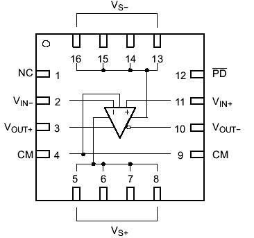
The THS4509 is offered in a Quad 16-pin leadless QFN package (RGT), and is characterized for operation over the full industrial temperature range from 40°C to 85°C.

 THS4508 Data Sheet


