THS3201

Features: Unity Gain Bandwidth: 1.8 GHz High Slew Rate: 10500 V/s Distortion at 100 MHz: (G = 10 V/V,RL = 100 , 2-VPP envelope) − IMD3: −80 dBc − OIP3: 41 dBmNoise Figure : 11 dB (G = 10 V/V,RG = 28 , RF = 255 )Input Referred Noise (f > 10 MHz) − Voltage Noise: 1.65 nV/...

product image

THS3201 Picture
SeekIC No. : 004518860 Detail

THS3201: Features: Unity Gain Bandwidth: 1.8 GHz High Slew Rate: 10500 V/s Distortion at 100 MHz: (G = 10 V/V,RL = 100 , 2-VPP envelope) − IMD3: −80 dBc − OIP3: 41 dBmNoise Figure : 11 dB ...

floor Price/Ceiling Price

Part Number:
THS3201
Supply Ability:
5000

Price Break

  • Qty
  • 1~5000
  • Unit Price
  • Negotiable
  • Processing time
  • 15 Days
Total Cost: $ 0.00

SeekIC Buyer Protection PLUS - newly updated for 2013!

  • Escrow Protection.
  • Guaranteed refunds.
  • Secure payments.
  • Learn more >>

Month Sales

268 Transactions

Rating

evaluate  (4.8 stars)

Upload time: 2025/1/12

Payment Methods

All payment methods are secure and covered by SeekIC Buyer Protection PLUS.

Notice: When you place an order, your payment is made to SeekIC and not to your seller. SeekIC only pays the seller after confirming you have received your order. We will also never share your payment details with your seller.
Product Details

Description


Features:

Unity Gain Bandwidth: 1.8 GHz
High Slew Rate: 10500 V/s
Distortion at 100 MHz: (G = 10 V/V,RL = 100 , 2-VPP envelope)
    − IMD3: −80 dBc
    − OIP3: 41 dBm
Noise Figure : 11 dB (G = 10 V/V,RG = 28 , RF = 255 )
Input Referred Noise (f > 10 MHz)
   − Voltage Noise: 1.65 nV/Hz
   − Noninverting Current Noise: 13.4 pA/Hz
   − Inverting Current Noise: 20 pA/Hz
Output Current: +115/−100 mA
Power Supply Voltage Range: ±3.3 V to ±7.5 V


Application

Arbitrary Waveform Driver
High-Resolution, High-Sampling Rate ADC Drivers
High-Resolution, High-Sampling Rate DAC Output Buffers
If Amplification for Wireless Communications Applciations
Broadcast Video and HDTV Line Drivers Low-Noise, Low-Distortion, Wideband Application Circuit                    


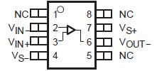
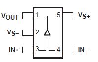
Pinout

  Connection Diagram  Connection Diagram


Specifications

  UNIT
Supply voltage, VS 16.5 V
Input voltage, VI ±VS
Output current, IO(2) 175 mA
Differential input voltage, VID ±3 V
Continuous power dissipation See Dissipation Rating Table
Maximum junction temperature, TJ (3) 150°C
Maximum junction temperature, continuous operation, long term reliability TJ (4) 125°C
Operating free-air temperature range, TA -40°C to 85°C
Storage temperature range, Tstg -65°C to 150°C
Lead temperature 1,6 mm (1/16 inch) from case for 10 seconds 300°C
ESD ratings: HBM 3000 V
CDM 1500 V
MM 100 V
(1) Stresses above these ratings may cause permanent damage.Exposure to absolute maximum conditions for extended periods may degrade device reliability. These are stress ratings only, and functional operation of the device at these or any other conditions beyond those specified is not implied.
(2) The THS3201 may incorporate a PowerPAD on the underside of the chip. This acts as a heat sink and must be connected to a thermally dissipative plane for proper power dissipation. Failure to do so may result in exceeding the maximum junction temperature which could permanently damage the device. See TI technical briefs SLMA002 and SLMA004 for more information about utilizing the PowerPAD thermally enhanced package.
(3) The absolute maximum temperature under any condition is limited by the constraints of the silicon process.
(4) The maximum junction temperature for continuous operation is limited by package constraints. Operation above this temperature may result in reduced reliability and/or lifetime of the device.


Description

The THS3201 is a wide-band, high-speed current-feedback amplifier, designed to operate over a wide supply range of ±3.3 V to ±7.5 V for todays high performance applications.

The wide supply range combined with distortion as low as −74 dBc at 10 MHz, plus an extremely high slew rate of 10500 V/s makes the THS3201 ideally suited for arbitrary waveform driver applications. The distortion performance also enables driving high-resolution and high-sampling rate ADCs. Moreover, the gain of +2 bandwidth of 850 MHz, combined with a 0.1 dB flatness of 380 MHz makes the THS3201 ideal for broadcast video and HDTV applications. The THS3201 also offers excellent performance for IF amplification in wireless communications systems by having IMD3 performance of −80 dBc, OIP3 of 41 dBm, and a noise figure of 11 dB, all at 100 MHz with a gain +10 V/V, while driving a 2-VPP envelope into a 100- load.


Customers Who Bought This Item Also Bought

Margin,quality,low-cost products with low minimum orders. Secure your online payments with SeekIC Buyer Protection.
Line Protection, Backups
Optoelectronics
Discrete Semiconductor Products
Fans, Thermal Management
View more