Features: Analog Supply 3 V
Digital Supply 3 V
Configurable Input Functions:
− Single Ended
− Differential
Differential Nonlinearity: ±0.45 LSB
Signal-to-Noise: 60 dB Typ f(IN) at 4.8 MHz
Spurious Free Dynamic Range: 72 dB
Adjustable Internal Voltage Reference
On-Chip Voltage Reference Generator
Unsigned Binary Data Output
Out-of-Range Indicator
Power-Down Mode Analog Supply 3 V
Digital Supply 3 V
Configurable Input Functions:
− Single Ended
− Differential
Differential Nonlinearity: ±0.45 LSB
Signal-to-Noise: 60 dB Typ f(IN) at 4.8 MHz
Spurious Free Dynamic Range: 72 dB
Adjustable Internal Voltage Reference
On-Chip Voltage Reference Generator
Unsigned Binary Data Output
Out-of-Range Indicator
Power-Down ModeApplication Video/CCD Imaging
Communications
Set-Top Box
Medical
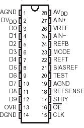
Pinout Specifications
Supply voltage range: AVDD to AGND, DVDD to DGND. . . . . . . . . . . . . . . . . . . . . −0.3 V to 4 V
AGND to DGND . . . . . . . . . . . . . . . . . . . . . . . . . . . . . . . . . . . . . . . . . . . . . . . . . . −0.3 V to 0.3 V
AVDD to DVDD . . . . . . . . . . . . . . . . . . . . . . . . . . . . . . . . . . . . . . . . . . . . . . . . . . . −4 V to 4 V
MODE input voltage range, MODE to AGND . . . . . . . . . . . . . . . . . . . . . . . . . . . .−0.3 V to AVDD + 0.3 V
Reference voltage input range, REFT, REFB, to AGND . . . . . . . . . . . . . . . . . . . . −0.3 V to AVDD + 0.3 V
Analog input voltage range, AIN to AGND . . . . . . . . . . . . . . . . . . . . . . . . . . . . −0.3 V to AVDD + 0.3 V
Reference input voltage range, VREF to AGND . . . . . . . . . . . . . . . . . . . . . . . . −0.3 V to AVDD + 0.3 V
Reference output voltage range, VREF to AGND . . . . . . . . . . . . . . . . . . . . . . . −0.3 V to AVDD + 0.3 V
Clock input voltage range, CLK to AGND . . . . . . . . . . . . . . . . . . . . . . . . . . . . .−0.3 V to AVDD + 0.3 V
Digital input voltage range, digital input to DGND . . . . . . . . . . . . . . . . . . . . . . .−0.3 V to DVDD + 0.3 V
Digital output voltage range, digital output to DGND . . . . . . . . . . . . . . . . . .−0.3 V to DVDD + 0.3 V
Operating junction temperature range, TJ . . . . . . . . . . . . . . . . . . . . . . . . . 0°C to 150°C
Storage temperature range, Tstg . . . . . . . . . . . . . . . . . . . . . . . . . . . . . . .−65°C to 150°C
Lead temperature 1,6 mm (1/16 in) from case for 10 seconds . . . . . . . . . 300°C
DescriptionThe THS1040 is a CMOS, low power, 10-bit, 40-MSPS analog-to-digital converter (ADC) that operates from a single 3-V supply. The THS1040 has been designed to give circuit developers flexibility. The analog input to the THS1040 can be either single-ended or differential. The THS1040 provides a wide selection of voltage references to match the user's design requirements. For more design flexibility, the internal reference can bebypassed to use an external reference to suit the dc accuracy and temperature drift requirements of the application. The out-of-range output indicates any out-of-range condition in THS1040's input signal.
The speed, resolution, and single-supply operation of the THS1040 are suited to applications in set-top-box (STB), video, multimedia, imaging, high-speed
acquisition, and communications. The speed and resolution ideally suit charge-couple device (CCD) input systems such as color scanners, digital copiers, digital cameras, and camcorders. A wide input voltage range allows the THS1040 to be applied in both imaging and communications systems.
The THS1040C is characterized for operation from 0°C to 70°C, while the THS1040I is characterized for operation from −40°C to 85°C.

 THS1040 Data Sheet


