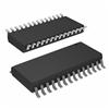
Features: Simultaneous Sampling of Two Single-Ended Signals or One Differential Signal
Integrated 16-Word FIFO
Signal-to-Noise and Distortion Ratio: 59 dB at fI = 2 MHz
Differential Nonlinearity Error: ±1 LSB
Integral Nonlinearity Error: ±1 LSB
Auto-Scan Mode for Two Inputs
3-V or 5-V Digital Interface Compatible
Low Power: 216 mW Max
5-V Analog Single Supply Operation
Internal Voltage References . . . 50 PPM/°C and ±5% Accuracy
Parallel µC/DSP Interface
Application Radar Applications
Communications
Control Applications
High-Speed DSP Front-End
Automotive Applications
Pinout Specifications
| |
THS10082 |
| Supply voltage range Su ly |
DGND to DVDD |
0.3 V to 6.5 V |
| BGND to BVDD |
0.3 V to 6.5 V |
| AGND to AVDD |
0.3 V to 6.5 V |
| Analog input voltage range |
AGND 0.3 V to AVDD + 1.5 V |
| Reference input voltage |
0.3 V + AGND to AVDD + 0.3 V |
| Digital input voltage range |
0.3 V to BVDD/DVDD + 0.3 V |
| Operating virtual junction temperature range, TJ |
40°C to 150°C |
| Operating free air temperature range T free-range, TA |
THS10082C |
0°C to 70°C |
| THS10082I |
40°C to 85°C |
| Storage temperature range, Tstg |
65°C to 150°C |
| Lead temperature 1,6 mm (1/16 inch) from case for 10 seconds |
260°C |
DescriptionThe THS10082 is a CMOS, low-power, 10-bit, 8 MSPS analog-to-digital converter (ADC). The speed, resolution, bandwidth, and single-supply operation of THS10082 are suited for applications in radar, imaging, high-speed acquisition, and communications. A multistage pipelined architecture with output error correction logic provides for no missing codes over the full operating temperature range. Internal control registers allow for programming the ADC into the desired mode. The THS10082 consists of two analog inputs, which are sampled simultaneously. These inputs can be selected individually and configured to single-ended or
differential inputs. An integrated 16 word deep FIFO allows the storage of data in order to take the load offof the processor connected to the ADC. Internal
reference voltages for the ADC (1.5 V and 3.5 V) are provided.
An external reference of THS10082 can also be chosen to suit the dc accuracy and temperature drift requirements of the application. Two different conversion modes can be selected. In the single conversion mode, a single and simultaneous conversion can be initiated by using the single conversion start signal (CONVST). The conversion clock in the single conversion mode is generated internally using a clock oscillator circuit. In the continuous conversion mode, an external clock signal is applied to the CONV_CLK input of the THS10082. The internal clock oscillator is switched off in the continuous conversion mode.
The THS10082C is characterized for operation from 0°C to 70°C, and the THS10082I is characterized for operation from 40°C to 85°C.

 THS10082 Data Sheet


