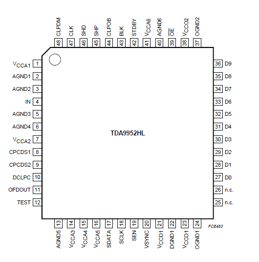
Features: · Sample rate = 25 Msps;10-bit resolution· Single 3.0 V supply operation (2.2 to 3.6 V operation for the digital outputs)· Low power consumption: only 115 mW at 2.7 V· Power consumption in standby mode: 4.5 mW (typical value)· Programmable gain amplifier: gain range = 36 dB in 0.1 dB ste...
TDA9952: Features: · Sample rate = 25 Msps;10-bit resolution· Single 3.0 V supply operation (2.2 to 3.6 V operation for the digital outputs)· Low power consumption: only 115 mW at 2.7 V· Power consumption in...
SeekIC Buyer Protection PLUS - newly updated for 2013!
268 Transactions
All payment methods are secure and covered by SeekIC Buyer Protection PLUS.
SYMBOL |
PARAMETER |
CONDITIONS |
MIN. |
MAX. |
UNIT |
VCCA |
analog supply voltage |
note 1 |
-0.3 |
+4.5 |
V |
VCCD |
digital supply voltage |
note 1 |
-0.3 |
+4.5 |
V |
VCCO |
digital outputs supply voltage |
note 1 |
-0.3 |
+4.5 |
V |
VCC |
supply voltage difference between VCCA and VCCD between VCCA and VCCO between VCCD and VCCO |
-0.5 -0.5 -0.5 |
+0.5 +1.2 +1.2 |
V V V | |
Vi |
input voltage |
referenced to AGND |
-0.3 |
+6.5 |
V |
Io |
data output current |
- |
±10 |
mA | |
Tstg |
storage temperature |
-55 |
+150 |
||
Tamb |
ambient temperature |
-20 |
+75 |
||
Tj |
junction temperature |
- |
150 |
The TDA9952 is a 10-bit analog-to-digital interface for CCD cameras. The device consists of a Correlated Double Sampling (CDS) circuit, a digitally Programmable Gain Amplifier (PGA), a black level clamp and a 10-bit Analog-to-Digital Converter (ADC).
An internal CDS input buffer is incorporated in order to avoid using an external buffer that would consume more power and therefore optimizing the application for low noise, low power working.
The PGA gain, the ADC clamp level and other settings are controlled via a 3-wire serial digital interface. An additional DAC is provided for system controls. The TDA9952 operates from a single 3 V power supply (2.7 V minimum) and dissipates 135 mW (typical value).