TDA9910

Features: 12-bit resolutionDirect IF sampling up to 370MHz90dB SFDR; 71dB SNR (f i=225MHz; B=5MHz)72dB SFDR; 66dB SNR (fi=175MHz; B=Nyquist)High-speed sampling rate up to 80Msample/sProgrammable acquisition output clock (complete conversion signaInternal front-end buffer (input capacitance below 1...

product image

TDA9910 Picture
SeekIC No. : 004517001 Detail

TDA9910: Features: 12-bit resolutionDirect IF sampling up to 370MHz90dB SFDR; 71dB SNR (f i=225MHz; B=5MHz)72dB SFDR; 66dB SNR (fi=175MHz; B=Nyquist)High-speed sampling rate up to 80Msample/sProgrammable acq...

floor Price/Ceiling Price

Part Number:
TDA9910
Supply Ability:
5000

Price Break

  • Qty
  • 1~5000
  • Unit Price
  • Negotiable
  • Processing time
  • 15 Days
Total Cost: $ 0.00

SeekIC Buyer Protection PLUS - newly updated for 2013!

  • Escrow Protection.
  • Guaranteed refunds.
  • Secure payments.
  • Learn more >>

Month Sales

268 Transactions

Rating

evaluate  (4.8 stars)

Upload time: 2025/1/12

Payment Methods

All payment methods are secure and covered by SeekIC Buyer Protection PLUS.

Notice: When you place an order, your payment is made to SeekIC and not to your seller. SeekIC only pays the seller after confirming you have received your order. We will also never share your payment details with your seller.
Product Details

Description


Features:

12-bit resolution
Direct IF sampling up to 370MHz
90dB SFDR; 71dB SNR (f i=225MHz; B=5MHz)
72dB SFDR; 66dB SNR (fi=175MHz; B=Nyquist)
High-speed sampling rate up to 80Msample/s
Programmable acquisition output clock (complete conversion signa
Internal front-end buffer (input capacitance below 1pF)
Full-scale controllable from 1.5V to 2V (p-p); continuous scale
Single 5V power supply
3.3V LVCMOS compatible digital outputs
Binary or two Os-complement LVCMOS output
CMOS compatible static digital inputs
Only 2clock cycles latency
Industrial temperature range from ?40 °C to +85°C
HTQFP48 package.


Application

2.5G and 3G cellular base infrastructure radio transceivers
Wireless access systems
Fixed telecommunication
Optical networking
WLAN infrastructure.


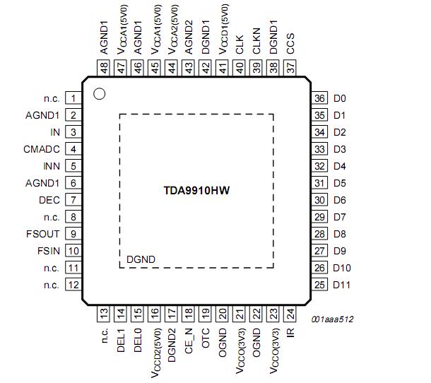
Pinout

  Connection Diagram


Specifications

SYMBOL PARAMETER CONDITIONS MIN MAX. UNIT
VCCA analog supply voltage -0.3 +7.0 V
VCCD digital supply voltage -0.3  +7.0  V
VCCO digital output supply voltage -0.3  +7.0  V
VCC supply voltage difference
 VCCA - VCCD
 VCCD-VCCO
 VCCA -VCCO
   -1.0
-1.0
-1.0
 +1.0
+4.0
+4.0
V
Vi input voltage referenced to AGND  -0.3  +7.0  V
Io output current    -  <tbd>  mA
Tstg storage temperature    -55  +150  °C
Tamb ambient temperature    -40  +85 °C
Tj junction temperature    -  150  °C


Description

   The TDA9910 is a 12-bit Analog-to-Digital Converter (ADC) optimized for direct IF sampling, and supporting the most demanding use conditions in ultra high IF radio transceivers for cellular infrastructure and other applications such as wireless access system, optical networking and  telecommunication. Thanks to its broadband input capabilities, the TDA9910 is ideal for single and multiple carriers data conversion.

  Operating at a maximum sampling rate of 80Msample/s, analog input signals are converted into 12-bit binary coded digital words. All static digital inputs are CMOS compatible. All output signals are LVCMOS compatible. The TDA9910 offers the most possible exible acquisition control system thanks to its programmable Complete Conversion Signal (CCS) that allows to adjust the delay of the acquisition clock.

  Thanks to its internal front-end buffer, the TDA9910 offers the lowest input capacitance (<1pF) and therefore the highestexibility in front-end aliasing strategy. Released in HTQFP48, it keeps the industry's smallest ADC of its category.


Customers Who Bought This Item Also Bought

Margin,quality,low-cost products with low minimum orders. Secure your online payments with SeekIC Buyer Protection.
Cables, Wires
Connectors, Interconnects
Fans, Thermal Management
Integrated Circuits (ICs)
View more