Features: 130MHz, ?3dB small signal bandwidthDigitally controlled gainTTL/CMOS compatible digital inputs (3.3or5V)TTL single ended or differential clock input with PECL compatibility24dB gain control rangeFive steps of 6dBplus6dB fixed gain30dB gain maximumHigh impedance differential inputsLow imp...
TDA9901: Features: 130MHz, ?3dB small signal bandwidthDigitally controlled gainTTL/CMOS compatible digital inputs (3.3or5V)TTL single ended or differential clock input with PECL compatibility24dB gain contro...
SeekIC Buyer Protection PLUS - newly updated for 2013!
268 Transactions
All payment methods are secure and covered by SeekIC Buyer Protection PLUS.
SYMBOL | PARAMETER | MIN | MAX. | UNIT |
VCCA | analog supply voltage | -0.3 | +7.0 | V |
VCCD | digital supply voltage | -0.3 | +7.0 | V |
VCCO | digital output supply voltage | -0.3 | +7.0 | V |
VCC | supply voltage difference between VCCA andVCCD between VCCD andV CCO |
-1.0 -1.0 |
+1.0 +4.0 |
V V |
Vi | input voltage | -0.3 | +7.0 | V |
Io | output current | - | 10 | mA |
Tstg | storage temperature | -55 | +150 | °C |
Tamb | ambient temperature | -40 | +75 | °C |
Tj | junction temperature | - | 150 | °C |
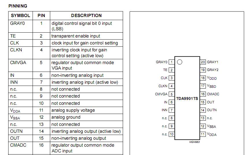
The TDA9901 is a wideband, low noise amplifier with differentialinputsandoutputs.TheTDA9901incorporates an AGC function with digital control.
The TDA9901 is optimized for fast switching between different gain settings, preserving small phase and amplitude error.
The TDA9901 presents an excellent combination of lownoise and good linearity for a wide input frequency range. The TDA9901 is optimized for processing IF signals in GSM base stations. It is also suited for many other applications as a general purpose digitally controlled variable gain amplifier.
The TDA9901 is able to operate from 4.75to5.25V supply for the analog part and from 3.0to5.25V for the digital part.