Features: ` Single-chip 5 V mixer/oscillator and synthesizer for TV and VCR tuners
` I2C-bus protocol compatible with 3.3 V and 5 V microcontrollers:
Address + 6 data bytes transmission
Address + 1 status byte (I2C-bus read mode)
Four independent I2C-bus addresses.
` Two PMOS open-drain ports with 5 mA source capability to switch high band and FM sound trap (P2 and P3)
` One PMOS open-drain port with 20 mA source capability to switch the mid band (P1)
` One PMOS open-drain port with 10 mA source capability to switch the low band (P0)
` Five step, 3-bit Analog-to-Digital Converter (ADC) and NPN open-collector general purpose port with 5 mA sinking capability (P6)
` NPN open-collector general purpose port with 5 mA sinking capability (P4)
` Internal AGC flag
` In-lock flag
` 33 V tuning voltage output
` 15-bit programmable divider
` Programmable reference divider ratio: 64, 80 or 128
` Programmable charge pump current: 60 or 280 mA
` Varicap drive disable
` Balanced mixer with a common emitter input for the low band (single input)
` Balanced mixer with a common base input for the mid and high bands (balanced input)
` 2-pin asymmetrical oscillator for the low band
` 2-pin asymmetrical oscillator for the mid band
` 4-pin symmetrical oscillator for the high band
` Frequency ranges: see Table 1
` IF preamplifier with asymmetrical 75 W output impedance to drive a SAW filter (500 W/40 pF)
` Wide-band AGC detector for internal tuner AGC:
Five programmable take-over points
Two programmable time constants.
Application· TV and VCR tuners
· Specially suited for switched concepts, all systems
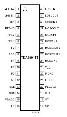
· Specially suited for strong off-air reception.Pinout
Specifications
| Symbol |
Parameter |
Conditions |
Min |
Max |
Unit |
| VCC |
supply voltage |
|
-0.3 |
+6 |
V |
| VXTAL |
crystal input voltage |
|
-0.3 |
VCC + 0.3 |
V |
| VP6/ADC |
NPN port input and output voltage |
|
-0.3 |
VCC + 0.3 |
V |
| IP6/ADC |
NPN port output current (open-collector) |
|
0 |
10 |
mA |
| VVT |
tuning voltage output |
|
-0.3 |
+35 |
V |
| VCP |
charge pump output voltage |
|
-0.3 |
VCC + 0.3 |
V |
| VP4 |
NPN port output voltage (open-collector) |
|
-0.3 |
VCC + 0.3 |
V |
| IP4 |
NPN port output current (open-collector) |
|
0 |
10 |
mA |
| VSDA |
serial data input/output voltage |
|
-0.3 |
+6 |
V |
| ISDA |
serial data output current |
|
-1 |
+10 |
mA |
| VSCL |
serial clock input voltage |
|
-0.3 |
+6 |
V |
| VAS |
address selection input voltage |
|
-0.3 |
VCC + 0.3 |
V |
| VPn |
PMOS port output voltage (open-drain) |
|
-0.3 |
VCC + 0.3 |
V |
| IP1 |
PMOS port output current (open-drain) |
|
-25 |
0 |
mA |
| IP0 |
PMOS port output current (open-drain) |
|
-15 |
0 |
mA |
| IP2, IP3 |
PMOS port output current (open-drain) |
|
-10 |
0 |
mA |
| Tstg |
storage temperature |
|
-40 |
+150 |
|
| Tamb |
ambient temperature |
|
-20 |
+85 |
|
| Tj |
junction temperature |
|
- |
150 |
|
DescriptionTDA6500TT and TDA6501TT are programmable 2-mixer, 3-oscillator and synthesizer MOPLL intended for pure 3-band tuner concepts (see Fig.1).
The TDA6500TT and TDA6501TT include two double balanced mixers for the low and mid/high bands and three oscillators for the low, mid and high bands respectively. The band limits for PAL tuners are shown in Table 1. Other functions are an IF amplifier, a wide-band AGC detector and a PLL synthesizer. Two pins of TDA6500TT and TDA6501TT are available between the mixer output and the IF amplifier input to enable IF filtering for improved signal handling.
Bit P0 enables Port P0 and the low band mixer and oscillator. Bit P1 enables Port P1, the mid/high band mixer and the mid band oscillator. Bit P2 enables Port P2 and bit P3 enables Port P3. When P0 and P1 are disabled, the mid/high band mixer and the high band oscillator are enabled.
The AGC detector TDA6500TT and TDA6501TT provides information about the IF amplifier level. Five AGC take-over points are available by software. Two programmable AGC time constants are available for search tuning and normal tuner operation. The synthesizer TDA6500TT and TDA6501TT consists of a 15-bit programmable divider, a crystal oscillator and its programmable reference divider and a phase/frequency detector combined with a charge pump, which drives the tuning amplifier including 33 V output.
Depending on the reference divider ratio (64, 80 or 128) the phase comparator operates at 62.50 kHz, 50.00 kHz or 31.25 kHz with a 4 MHz crystal.
The TDA6500TT and TDA6501TT can be controlled according to the I2C-bus format. The lock detector bit FL is set to logic 1 when the loop is locked. The AGC bit is set to logic 1 when the internal AGC is active (level below 3 V). These two flags of TDA6500TT and TDA6501TT are read on the SDA line (status byte) during a read operation (see Table 8).
The ADC input of TDA6500TT and TDA6501TT is available on pin P6/ADC for digital AFC control. The ADC code is read during a read operation (see Table 8). In test mode, pin P6/ADC is used as a test output for 1/2fref and 1/2fdiv (see Table 5).
A minimum of seven bytes, including address byte, TDA6500TT and TDA6501TT are required to address the device, select the VCO frequency, program the ports, set the charge pump current, set the reference divider ratio, select the AGC take-over point and select the AGC time constant. The TDA6500TT and TDA6501TT have four independent I2C-bus addresses which can be selected by applying a specific voltage on input AS (see Table 4).

 TDA6501TT Data Sheet


