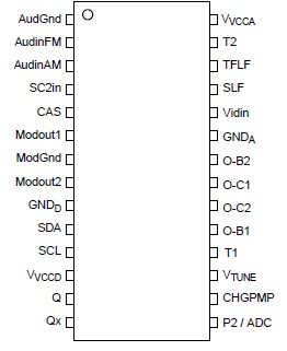
Features: · Frequency and amplitude-stable balanced oscillator for the VHF, Hyper band and the UHF frequency range
· Clamped video input with peak white level detection for I2C bus controlled gain setting of the video amplifier
· Programmable sound carriers 4.5 MHz, 5.5 MHz, 6 MHz, 6.5 MHz
· Second sound carrier input
· Balanced RF output
· Low-noise reference voltage
· 1-chip system for mC control (I2C bus)
· Fast I2C bus mode possible
· 4 programmable chip addresses
· Smallest possible lock-in time; no asynchronous divider stage
· Short pull-in time for quick channel switch-over and optimized loop stability
· One high-current switch output
· 5-level A/D converter
· Lock-in flag
· Power-down flag
· Few external components
· Package TSSOP 28
· 5 V supply voltage
ApplicationThe TDA 6060XS is suitable for all modulator boxes
The TDA 6060G has modified divider ratio for applications with +125kHz RF frequency offset (e.g. 38.875MHz, N=620+2) and reduced Sound Carrier Levels.
Pinout Specifications
| Parameter |
Symbol |
Limit Values |
Unit |
Remarks |
| min |
max |
| Supply voltage |
VVCCD |
-0.3 |
+6 |
V |
|
| Output CHGPMP |
VCHGPMP |
-0.3 |
+3.5 |
V |
|
| Crystal oscillator pins Q, Qx |
VQ |
-0.3 |
VVCCD |
V |
|
| Bus input/output SDA |
VSDA |
-0.3 |
+6 |
V |
|
| Bus input SCL |
VSCL |
-0.3 |
+6 |
V |
|
| Chip address switch CAS |
VCAUS |
-0.3 |
VVCCD |
V |
|
| Output active filter VTUNE |
VTUNE |
-0.3 |
+35 |
V |
|
| Bus output SDA |
ISDAL |
0 |
5 |
mA |
open collector |
| Port output P2 |
IPL |
0 |
20 |
mA |
open collector |
| Port output P2 |
VP |
-0.3 |
+6 |
V |
|
DescriptionThe modulator section TDA6060G includes a gain adjustable video amplifier, a double balanced mixer working as a AM video modulator for positive or negative modulation, a balanced oscillator for VHF, Hyper band and UHF, a sound modulator TDA6060G suitable for FM and AM modulation, a programmable sound carrier oscillator and a reference voltage source.
The audio signal TDA6060G is coupled to the gain settable audio pre-amplifier of the FM AF input (AudinFM) and to the AM input amplifier (AudinAM). The pre-emphasis is done with an external circuitry in front of the FM audio input. The FM audio amplifier allows a gain setting in four steps with the AU0 / 1 bits in the negative video modulation mode (PN = 0). The amplified audio signal TDA6060G is fed to the FM modulator. The modulated sound carrier is filtered by a tracked bandpass filter and added to the video signal. In the positve video modulation mode the the audio signal is directly fed to the AM sound modulator. The sound carriers are generated by a programmable on chip oscillator. The four possible frequencies are 4.5, 5.5, 6.0 and 6.5 MHz (2bit). To increase the speed of the sound PLL the loop filter current TDA6060G can be switched to 5I with the audio mode bits (table4). A second FM or NICAM sound carrier may be added via the input SC2in to the internally generated carrier.The SC2in input is referenced to Audgnd and can be switched off by connecting SC2in to the supply voltage.
The positve video signal TDA6060G is capacitively coupled to the video input pin (Vidin). An internal clamping circuit is referenced to the sync tip level. If the video signal exceeds the maximum level the peak white level is clipped. The clipping circuit acts also as a detector and sets a flag (FLV) for the I2C bus. The video input amplifier TDA6060Gallows a gain setting in four steps. The polarity of the video signal can be switched for positve or negative modulation. The setting to positve modulation is combined with the AM modulation of the sound carrier. For the residual carrier adjustment a sawtooth test picture is used when the video modulator is in overmodulation mode.TDA6060G is active by conneting test pin T1 to ground.
The adjustments of the modulation depth and the picture to sound carrier ratio of TDA6060G can be done in four steps.
The RF oscillator of TDA6060G works as gain controlled LC tuned astable multivibrator. The output of the oscillator is decoupled by two isolation amplifiers, one for the modulator mixer and one for the synthesizer PLL. The VCO TDA6060G can be switched off by setting both audio mode bits to 1 in positive modulation mode (table 4) The added sound carrier and video signals are mixed with the RF oscillator signal in the double balanced mixer and then fed to both RF outputs (Modout1 / Modout2)

 TDA6060G Data Sheet


