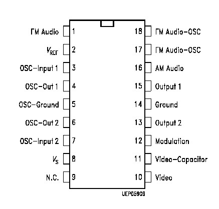
Features: ·FM-audio modulator·Sync level clamping of video input signal·Controlling of peak white value·Continuous adjustment of modulation depth for positive or negative values·Symmetrical mixer output with separate ground area·Symmetrical oscillator with separate RF-ground·Low spurious radiation...
TDA5666-5: Features: ·FM-audio modulator·Sync level clamping of video input signal·Controlling of peak white value·Continuous adjustment of modulation depth for positive or negative values·Symmetrical mixer ou...
SeekIC Buyer Protection PLUS - newly updated for 2013!
268 Transactions
All payment methods are secure and covered by SeekIC Buyer Protection PLUS.
Parameter |
Symbol |
Limit Values |
Unit |
Remarks | ||
min. |
typ. |
max. | ||||
Supply voltage pin 8 Current from pin 2 Voltage at pin 1 Voltage at pin 2 Voltage at pin 10 Capacitance at pin 2 Capacitance at pin 11 Voltage at pin 12 Voltage at pin 13 Voltage at pin 15 Voltage at pin 16 |
VS I2 V1 V2 V10 C2 C11 V12 V13 V15 V16 |
0.3 0 0 6 0 0 0 0.3 V2 V2 V2 -1.5 |
14.5 2 2 8.5 1.5 100 15 1.4 VS VS VS+1.5 |
V mA V V Vpp nF mF V V V V |
V2= 7-8 V VS = 10-13.5 V only via C (max. 1 mF) VS = 10-13.5 V | |
According to the application circuit, only the provided circuitry can be connected to pins 3,4,6,7,17 and 18. | ||||||
Junction temperature Storage temperature Thermal resistance |
Tj Tstg Rth |
40 | 150 125 80 |
oC oC K/W |
Oscillator
The RF-oscillator TDA5666-5 is available at pins 3-7. The oscillator operates as a symmetrical Colpitts circuit. The oscillator chip ground, pin 5, should be connected to ground at the resonance circuit shielding point. An external oscillator TDA5666-5 can be injected inductively or capacitively via pins 3 and 7. The layout of the PCB should be such as to provide a minimum shielding attenuation between the oscillator pins 3-7 and modulator output pins 13-15 of approximately 80 dB.
For optimal residual carrier suppression, the symmetrical mixer outputs TDA5666-5 at pins 13, 15 should be connected to a matched balanced-to-unbalanced broadband transformer, e.g. a Guanella transformer with good phase precision at 0o and 180o. The transmission loss should be less than 3 dB. In addition, an LC-low pass filter combination is required at the output. The cut-off frequency of the low pass filter combination must exceed the maximum operating frequency.
Video
The video signal of TDA5666-5 with the negative synchronous level is capacitively connected to pin 10. The internal clamping circuit is referenced to the synchronizing level. Should the video signal change by 6 dB, this change will be compensated by the resonance circuit which is set by the peak white value. At pin 11, the current pulses of the peak white detector are filtered through the capacitor which also determines the control time constant. The RFcarrier TDA5666-5 switches from negative to positive video modulation, when pin 12 is connected to ground. By varying the value of resistance R at pin 12 between ¥ ... 0 W the modulation depth TDA5666-5 can be increased from 70% to 100% when the modulation is negative and decreased from 100% to 70% when the modulation is positive.
Audio
Via pin 1, the audio signal TDA5666-5 is capacitively coupled to the AF-input for the FM-modulation of the oscillator. A parallel resonance circuit is connected to the audio carrier oscillator at pins 17, 18. The unloaded Q of the resonant circuit must be Q = 25 and the parallel resistor RT = 8.2 kW to ensure a video to audio carrier ratio of 12.5 dB. At the same time, the capacitative and/or inductive reactance for the resonance frequency should have a value of XC » XL » 800 . The video to audio carrier ratio can be changed by connecting an external voltage to pin 16, TDA5666-5 deviates from the internal reference voltage. At the output of the above described mixer the FM modulated audio signal is added to the video signal and mixed with the oscillator signal in the RF-mixer.
Source
The internal reference voltage of TDA5666-5 is available at pin 2 and has to be capacitively blocked there.