Features: · Designed for 10 dual-stripe MR-read/inductive write heads
· Current bias-current sense architecture
· Single supply voltage (5.0 V ±10%); a separate write drivers supply pin can be biased from VCC to 8 V +10%
· MR elements connected to ground (GND)
· Equal bias currents in the two MR stripes of each head
· On-chip AC couplings eliminate MR head DC offset
· 3-wire serial interface for programming
· Programmable voltage/current mode write data input
· Programmable high frequency zero-pole gain boost
· Programmable write driver compensation capacitance
· Programmable MR bias currents and write currents
· 1-bit programmable read gain
· Sleep, standby, active and test modes available
· Measurement of head resistances in test mode
· In test mode, one MR bias current may be forced to a minimum current
· Short write current rise and fall times with near rail-to-rail voltage swing
· Head unsafe pin for signalling of abnormal conditions and behaviour
· Low supply voltage write current inhibit (active or inactive)
· Support servo writing
· Provide temperature monitor
· Thermal asperity detection with programmable threshold level
· Requires only one external resistor.
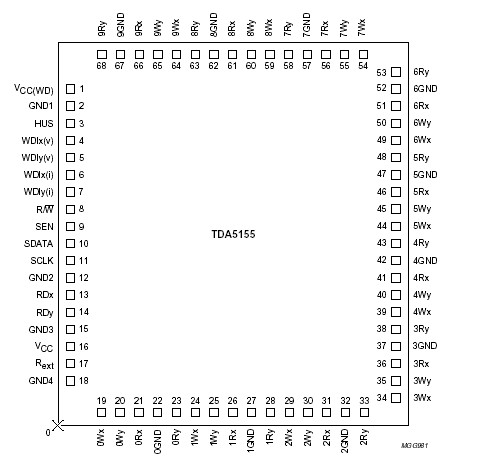
Application· Hard Disk Drive (HDD).Pinout Specifications
| SYMBOL |
PARAMETER |
MIN. |
MAX. |
UNIT |
| VCC |
supply voltage |
-0.5 |
+6.0 |
V |
| VCC(WD) |
write driver supply voltage |
-0.5 |
+9.5 |
V |
| Vn1 |
voltage on all pins except VCC, read inputs nRx, nRy and
write outputs nWx, nWy (n = 0 to 9)
but not higher than |
-0.5
|
+5.5
|
V
|
| - |
VCC + 0.5 |
V |
| Vn2 |
voltage on write driver outputs nWx, nWy
but not higher than |
-0.5
|
+8.8
|
V
|
| - |
VCC(WD) + 0.8 |
V |
| Vn3 |
voltage on read inputs nRx, nRy |
-0.5 |
+1 |
V |
| InGND |
current through pins nGND |
- |
0.1 |
A |
Tstg
|
storage temperature |
-65 |
+150 |
|
| Tj |
junction temperature |
- |
150 |
|
DescriptionThe 5.0 V pre-amplifier for HDD applications of TDA5155 has been designed for five terminal, dual-stripe Magneto-Resistive (MR)-read/inductive write heads. The disks of the disk drive are connected to ground.
To avoid voltage breakthrough between the heads and the disk, the MR elements of the heads are also connected to ground. The symmetry of the dual-stripe head-amplifier combination automatically distinguishes between the differential signals such as signals and the common-mode effects like interference. The latter are rejected by the amplifier.
The TDA5155 incorporates read amplifiers, write amplifiers, a serial interface, digital-to-analog converters, reference and control circuits which all operate on a single supply voltage of 5 V ±10%. The output drivers of TDA5155 have a separate supply voltage pin which can be connected to a higher supply voltage of up to 8 V +10%. The complementary output stages of the write amplifier allow writing with near rail-to-rail peak voltages across the inductive write head.
The read amplifier TDA5155 has low input impedance. The DC offset between the two stripes of the MR head is eliminated using on-chip AC coupling. Fast settling features are used to keep the transients short. As an option, the read amplifier TDA5155 may be left biased during writing so as to reduce the duration of these transients even further. Series inductance in the leads between the amplifier and MR heads influences the bandwidth which can be compensated by using a programmable high frequency gain boost (HF zero). HF noise and bandwidth can be attenuated using a programmable high frequency gain attenuator (HF pole).
On-chip digital-to-analog converters for MR bias currents and write currents TDA5155 are programmed via a 3-wire serial interface. Head selection, mode control, testing and servo writing TDA5155 can also be programmed using the serial interface. In sleep mode the CMOS serial interface is operational. Fig.1 shows the block diagram of the device.

 TDA5155 Data Sheet


