TDA5153

Features: · Designed for 4 (TDA5153BG) or 6 dual-stripe MR-read/inductive write heads· Current bias-current sense architecture· Single supply voltage (5.0 V ±10%); a separate write drivers supply pin can be biased from VCC to 8 V +10%· MR elements connected to ground (GND)· Equal bias currents in ...

product image

TDA5153 Picture
SeekIC No. : 004516432 Detail

TDA5153: Features: · Designed for 4 (TDA5153BG) or 6 dual-stripe MR-read/inductive write heads· Current bias-current sense architecture· Single supply voltage (5.0 V ±10%); a separate write drivers supply pi...

floor Price/Ceiling Price

Part Number:
TDA5153
Supply Ability:
5000

Price Break

  • Qty
  • 1~5000
  • Unit Price
  • Negotiable
  • Processing time
  • 15 Days
Total Cost: $ 0.00

SeekIC Buyer Protection PLUS - newly updated for 2013!

  • Escrow Protection.
  • Guaranteed refunds.
  • Secure payments.
  • Learn more >>

Month Sales

268 Transactions

Rating

evaluate  (4.8 stars)

Upload time: 2025/1/12

Payment Methods

All payment methods are secure and covered by SeekIC Buyer Protection PLUS.

Notice: When you place an order, your payment is made to SeekIC and not to your seller. SeekIC only pays the seller after confirming you have received your order. We will also never share your payment details with your seller.
Product Details

Description


Features:

· Designed for 4 (TDA5153BG) or 6 dual-stripe MR-read/inductive write heads
· Current bias-current sense architecture
· Single supply voltage (5.0 V ±10%); a separate write drivers supply pin can be biased from VCC to 8 V +10%
· MR elements connected to ground (GND)
· Equal bias currents in the two MR stripes of each head
· On-chip AC couplings eliminate MR head DC offset
· 3-wire serial interface for programming
· Programmable high-frequency zero-pole gain boost
· Programmable write driver compensation capacitance
· Programmable MR bias currents and write currents
· 1-bit programmable read gain
· Sleep, standby, active and test modes available
· Measurement of head resistances in test mode
· In test mode, one MR bias current may be forced to a minimum current
· Short write current rise and fall times with near rail-to-rail voltage swing
· Head unsafe pin for signalling of abnormal conditions and behaviour
· Low supply voltage write-current inhibit (active or inactive)
· Supports servo writing
· Provides temperature monitor
· Thermal asperity detection with programmable threshold level
· Requires only one external resistor.


Application

· Hard Disk Drive (HDD).


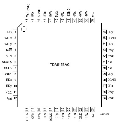
Pinout

  Connection Diagram


Specifications

SYMBOL PARAMETER MIN. MAX. UNIT
VCC supply voltage -0.5 +6.0 V
VCC(WD) write driver supply voltage -0.5 +9.5 V
VIL
LOW level digital input voltage
-0.5 +5.5 V
VIH HIGH level digital input voltage -0.5 +5.5 V
Vn1 voltage on all pins except VCC, read inputs nRx, nRy and
write outputs nWx, nWy (n = 0 to 9)
but not higher than
-0.5
-
+5.5
VCC + 0.5
V
V
Vn2 voltage on write driver outputs nWx, nWy
but not higher than
-0.5
-
+8.8
VCC(WD) + 0.8
V
V
Vn3 voltage on read inputs nRx, nRy -0.5 1 V
InGND current through pins nGND - 0.1 A
Tstg
storage temperature
-65
+150
Tj junction temperature - 150


Description

The 5.0 V pre-amplifier TDA5153 for HDD described here is designed for five terminals, dual stripe Magneto-Resistive (MR)-read/inductive-write heads. The disks of the disk drive are connected to ground. To avoid voltage break-through between the heads and the disk, the MR elements of the heads are also connected to ground. The symmetry of the dual-stripe head-amplifier combination automatically distinguishes between the differential signals such as signals and the common-mode effects like interference. The latter are rejected by the amplifier.

The TDA5153 incorporates read amplifiers, write amplifiers, serial interface, digital-to-analog converters, reference and control circuits which operate on a single supply voltage of 5 V ±10%. The output drivers have a separate supply voltage pin, TDA5153 can be connected to a higher supply voltage of up to 8 V +10%. The complementary output stages of the write amplifier allow writing with near rail-to-rail peak voltages across the inductive write head.

The read amplifier TDA5153 has a low input impedance. The DC offset between the two stripes of the MR head is eliminated using on-chip AC coupling. Fast settling features are used to keep the transients short. As an option, the read amplifier TDA5153 may be left biased during writing so as to reduce the duration of these transients even more. Series inductance in the leads between the amplifier and MR heads influences the bandwidth which can be compensated by using a programmable high-frequency gain-boost (HF zero). HF noise and bandwidth can be attenuated using a programmable high-frequency gain-attenuator (HF pole).

On-chip digital-to-analog converters for MR bias currents and write currents TDA5153 are programmed via a 3-wire serial interface. Head selection, mode control, testing and servo writing can also be programmed using the serial interface. In sleep mode the CMOS TDA5153 serial interface is operational. Figure 1 shows the block diagram of the device.


Customers Who Bought This Item Also Bought

Margin,quality,low-cost products with low minimum orders. Secure your online payments with SeekIC Buyer Protection.
Cables, Wires - Management
Batteries, Chargers, Holders
Industrial Controls, Meters
Cable Assemblies
Soldering, Desoldering, Rework Products
Integrated Circuits (ICs)
View more