Features: ` Voltage output
` Space saving packages SO8 or DIP8
` Low power consumption
` Wide dynamic range (16-bit resolution)
` Continuous Calibration (CC) concept
` Easy application:
single 4 to 5.5 V rail supply
output current and bias current are proportional to the supply voltage
integrated current-to-voltage converter
` Fast settling time permits 2, 4 and 8 * oversampling (serial input) or double-speed operation at 4 * oversampling
` Internal bias current ensures maximum dynamic range
` Wide operating temperature range (-40 °C to +85 °C)
` Compatible with most current Japanese input formats: time multiplexed, two's complement, TTL
` No zero-crossing distortion
` Cost efficient.
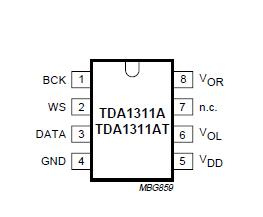
Pinout Specifications
| SYMBOL |
PARAMETER |
CONDITIONS |
MIN. |
MIN. |
UNIT |
| VP |
positive supply voltage |
|
- |
6.0 |
V |
| Txtal(max) |
maximum crystal temperature |
|
-55 |
+150 |
°C |
| Tstg |
storage temperature |
|
- |
+150 |
°C |
| Tamb |
operating ambient temperature |
|
-40 |
+85 |
°C |
| Ves |
electrostatic handling |
note 1 |
-2000 |
+2000 |
V |
| note 2 |
-200 |
+200 |
V |
Note
1. Human body model: C = 100 pF, R = 1500 , 3 pulses positive and 3 pulses negative.
2. Machine model: C = 200 pF, L = 0.5 mH, R = 10 , 3 pulses positive and 3 pulses negative.
DescriptionThe TDA1311A; AT is a voltage-driven digital-to-analog converter and is new generation of DAC devices which embodies the innovative technique of Continuous Calibration (CC). The largest bit-currents are repeatedly generated by one single current reference source. This duplication is based upon an internal charge storage principle which has an accuracy insensitive to ageing, temperature matching and process variations.
The TDA1311A; AT is fabricated in a 1.0 mm CMOS process and features an extremely low-power dissipation, small package size and easy application. Furthermore, the accuracy of the intrinsic high coarse-current combined with the implemented symmetrical offset decoding method preclude zero-crossing distortion and ensures high quality audio reproduction. Therefore, the CC-DAC is eminently suitable for use in (portable) digital audio equipment.

 TDA1311A Data Sheet


