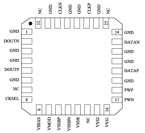
Features: `Operation to 12.5 Gbits/s NRZ.` Internal optional retiming flip-flop to minimize output data pattern jitter.` Adjustable output amplitude up to 3 V (RL = 50 ).` Integrated dc level adjustment to 1.5 V` Complementary data and clock inputs, and data output.` Complete operation and control...
TCMD0110G: Features: `Operation to 12.5 Gbits/s NRZ.` Internal optional retiming flip-flop to minimize output data pattern jitter.` Adjustable output amplitude up to 3 V (RL = 50 ).` Integrated dc level adjust...
SeekIC Buyer Protection PLUS - newly updated for 2013!
268 Transactions
All payment methods are secure and covered by SeekIC Buyer Protection PLUS.
Parameter |
Symbol |
Min |
Max |
Unit |
Storage Temperature |
Tstg |
-40 |
125 |
°C |
Supply Voltage |
Vss |
-5.5 |
0 |
V |
Supply Current |
Iss |
- |
400 |
mA |
Input Voltage |
VDATAP, VDATAN |
-2.0 |
0.5 |
V |
Output Voltage |
VDOUTP, VDOUTN |
-4.1 |
0.5 |
V |
Modulation Control Voltage |
VMOD |
Vss 0.5 |
Vss + 1.5 |
V |
Offset Control Voltage |
VBIAS |
Vss 0.5 |
Vss + 2.5 |
V |
Pulse Width Control Voltage |
VPWP, VPWN |
Vss 0.5 |
Vss + 2.5 |
V |
Modulation Current |
IVMOD |
-3 |
3 |
mA |
The TCMD0110G has been designed to drive electroabsorption modulators (EAMs), electroabsorption modulated lasers (EMLs), Mach-Zehnder (M-Z) lithium niobate modulators, and direct modulated lasers (DMLs) that have a 50 input impedance at speeds up to 12.5 Gbit/s NRZ. For nonclocked applications,a clock disable pin is provided.
The driver consists of an input buffer TCMD0110G, a limiting amplifier, a selectable data retiming section, a pulse width control circuitry, an output buffer with adjustable modulation level, and a dc offset section to provide a mark level adjustment.
The output buffer is designed to provide 3 V of modulation to a 50 load at each output. The dc offset adjustment networks provide down to 1.5 V offset (see Figure 7). The dc offset for the unused output can be disabled to minimize power consumption (see Table 1).
The input data TCMD0110G is retimed using an integrated flip-flop to remove incoming pattern dependent jitter. This feature is enabled using a clock select pad (see Table 1). If no clock is available, the TCMD0110G can be operated in a nonclocked mode.
The unused output can be terminated through the integrated 50 resistor when using the die form of the product(see Table 1).