TC7WG00FC

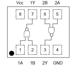
Features: • High-level output current: IOH/IOL = ±8 mA (min)at VCC = 3 V• High-speed operation: tpd = 2.5 ns (typ.) at VCC = 3.3 V,15pF• Operating voltage range: VCC = 0.9~3.6 V• 5.5-V tolerant inputs• 3.6-V power down protection outputsPinoutSpecifications Char...

product image

TC7WG00FC Picture
SeekIC No. : 004515054 Detail

TC7WG00FC: Features: • High-level output current: IOH/IOL = ±8 mA (min)at VCC = 3 V• High-speed operation: tpd = 2.5 ns (typ.) at VCC = 3.3 V,15pF• Operating voltage range: VCC = 0.9~3.6 V&#...

floor Price/Ceiling Price

Part Number:
TC7WG00FC
Supply Ability:
5000

Price Break

  • Qty
  • 1~5000
  • Unit Price
  • Negotiable
  • Processing time
  • 15 Days
Total Cost: $ 0.00

SeekIC Buyer Protection PLUS - newly updated for 2013!

  • Escrow Protection.
  • Guaranteed refunds.
  • Secure payments.
  • Learn more >>

Month Sales

268 Transactions

Rating

evaluate  (4.8 stars)

Upload time: 2025/1/12

Payment Methods

All payment methods are secure and covered by SeekIC Buyer Protection PLUS.

Notice: When you place an order, your payment is made to SeekIC and not to your seller. SeekIC only pays the seller after confirming you have received your order. We will also never share your payment details with your seller.
Product Details

Description


Features:

• High-level output current: IOH/IOL = ±8 mA (min) 
                                            at VCC = 3 V
• High-speed operation: tpd = 2.5 ns (typ.)
                                       at VCC = 3.3 V,15pF
• Operating voltage range: VCC = 0.9~3.6 V
• 5.5-V tolerant inputs
• 3.6-V power down protection outputs


Pinout

  Connection Diagram


Specifications

Characteristics Symbol Ratingh Unit
Power supply viltage VCC −0.5~4.6 V
DC input voltage VIN −0.5~7.0 V
DC output voltage VOUT −0.5~4.6              (Note 1) V
−0.5~VCC + 0.5   (Note 2)
Input diode current IIK −20 mA
Output diode current IOK −20                      (Note 3) mA
DC output current IOUT ±25 mA
DC VCC/GND current ICC ±50 mA
Power dissipation PD 150                     (Note 4) mW
Storage temperature Tstg −65~150 °C

Note: Using continuously under heavy loads (e.g. the application of high temperature/current/voltage and the significant change in temperature, etc.) may cause this product to decrease in the reliability significantly even if the operating conditions (i.e. operating temperature/current/voltage, etc.) are within the absolute maximum ratings and the operating ranges. Please design the appropriate reliability upon reviewing the Toshiba Semiconductor Reliability Handbook ("Handling Precautions"/Derating Concept and Methods) and individual reliability data (i.e. reliability test report and estimated failure rate, etc).
Note 1: VCC = 0V
Note 2: High or Low State. IOUT absolute maximum rating must be observed.
Note 3: VOUT < GND
Note 4: Mounted on an FR4 board.
            (25.4 mm * 25.4 mm * 1.6 t, Cu Pad: 11.56 mm2)


Customers Who Bought This Item Also Bought

Margin,quality,low-cost products with low minimum orders. Secure your online payments with SeekIC Buyer Protection.
Semiconductor Modules
Audio Products
Sensors, Transducers
Prototyping Products
DE1
Programmers, Development Systems
Cable Assemblies
View more