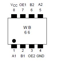
Features: • Operating voltage: VCC = 2~5.5 V• High speed operation: tpd = 0.25 ns (max)• Ultra-low on resistance: RON = 5 (typ.)• Electro-static discharge (ESD) performance: ±200 V or more (JEITA) ±2000 V or more (MIL)• High noise margin: VNIL = VNIH = 28% VCC (min)&...
TC7WB66FK: Features: • Operating voltage: VCC = 2~5.5 V• High speed operation: tpd = 0.25 ns (max)• Ultra-low on resistance: RON = 5 (typ.)• Electro-static discharge (ESD) performance:...
SeekIC Buyer Protection PLUS - newly updated for 2013!
268 Transactions
All payment methods are secure and covered by SeekIC Buyer Protection PLUS.
Characteristics |
Symbol |
Rating |
Unit | |
Power supply voltage |
VCC |
−0.5~7.0 |
V | |
Control pin input voltage |
VIN |
−0.5~7.0 |
V | |
Switch terminal I/O voltage |
VS |
−0.5~VCC + 0.5 |
V | |
Clump diode current | Control input pin |
IIK |
−50 |
mA |
Switch terminal |
±50 | |||
Switch I/O current |
IS |
128 |
mA | |
Power dissipation |
PD |
200 |
mW | |
DC VCC/GND current |
ICC/IGND |
±100 |
mA | |
Storage temperature |
Tstg |
−65~150 |
°C |
The TC7WB66FK is a low on-resistance, high-speed CMOS2-bit bus switch. This bus switch allows the connections or disconnections to be made with minimal propagation delay while maintaining Low power dissipation which is the feature of CMOS.
When output enable (OE) of TC7WB66FK is at High level, the switch is on; when at Low level, the switch is off.
P-MOS and N-MOS channel block means the TC7WB66FK is suitable for analog signal transmission.
All inputs of TC7WB66FK are equipped with protector circuits to protect the device from static discharge.