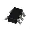
Type
:
Supply Current
:
Maximum Operating Temperature
: + 85 C
Mounting Style
: SMD/SMT
Supply Voltage - Max
: 2.7 V, 3.6 V
Supply Voltage - Min
: 1.1 V, 1.65 V
Propagation Delay Time
: 43 ns
Package / Case
: UF-6
Features: • Level converter for interfacing 1.2-V to 1.8-V, 1.2-V to 2.5-V, 1.2-V to 3.3-V, 1.5-V to 2.5-V, 1.5-V to 3.3-V, 1.8-V
to 2.5-V, 1.8-V to 3.3-V or 2.5 V to 3.3-V system.
• High-speed operation : tpd = 13.7 ns (max) (VCCA = 2.5 ± 0.2 V, VCCB = 3.3 ± 0.3 V)
tpd = 14.8 ns (max) (VCCA = 1.8 ± 0.15 V, VCCB = 3.3 ± 0.3 V)
tpd = 16.0 ns (max) (VCCA = 1.5 ± 0.1 V, VCCB = 3.3 ± 0.3 V)
tpd = 29 ns (max) (VCCA = 1.2 ± 0.1 V, VCCB = 3.3 ± 0.3 V)
tpd = 18.5 ns (max) (VCCA = 1.8 ± 0.15 V, VCCB = 2.5 ± 0.2 V)
tpd = 19.7 ns (max) (VCCA = 1.5 ± 0.15 V, VCCB = 2.5 ± 0.2 V)
tpd = 33 ns (max) (VCCA = 1.2 ± 0.15 V, VCCB = 2.5 ± 0.2 V)
tpd = 43 ns (max) (VCCA = 1.2 ± 0.1 V, VCCB = 1.8 ± 0.15 V)
• Output current : IOH/IOL = ±3 mA (min) (VCC = 3.0 V)
IOH/IOL = ±2mA (min) (VCC = 2.3 V)
IOH/IOL = ±0.5 mA (min) (VCC = 1.65 V)
• Latch-up performance: -300 mA
• ESD performance: Machine model ±200 V Human body model ±2000 V
• Ultra-small package: UF6
• Low current consumption : Using the new circuit significantly reduces current consumption when OE = "H".
Suitable for battery-driven applications such as PDAs and cellular phones.
• 3.6-V tolerant function and power-down protection provided on all inputs and outputs.Pinout Specifications
| Characteristics |
Symbol |
Rating |
Unit |
| Power supply voltage (Note 2) |
VCCA |
−0.5 to 4.6 |
V |
| VCCB |
−0.5 to 4.6 |
V |
DC input voltage
(A1, OE ) |
VIN |
−0.5 to 4.6 |
V |
DC output voltage −0.5 to 4.6 (Note 3)
(B1) |
VOUTB |
−0.5 to 4.6(Note 3) |
V |
| −0.5 to VCCB + 0.5 (Note 4) |
| Input diode current |
IIk |
-25 |
mA |
| Output diode current |
IOK |
±50 (Note 5) |
mA |
| DC output current |
IOUTB |
±6 |
mA |
| DC VCC/ground current per supply pin |
ICCA |
±25 |
mA |
| ICCB |
±50 |
mA |
| Power dissipation |
PD |
100 |
mW |
| Storage temperature |
Tstg |
−65 to 150 |
|
Note 1: Exceeding any of the absolute maximum ratings, even briefly, lead to deterioration in IC performance or
even destruction.
Using continuously under heavy loads (e.g. the application of high temperature/current/voltage and the
significant change in temperature, etc.) may cause this product to decrease in the reliability significantly
even if the operating conditions (i.e. operating temperature/current/voltage, etc.) are within the absolute
maximum ratings and the operating ranges.
Please design the appropriate reliability upon reviewing the Toshiba Semiconductor Reliability Handbook
("Handling Precautions"/"Derating Concept and Methods") and individual reliability data (i.e. reliability test
report and estimated failure rate, etc).
Note 2: Don't supply a voltage to VCCB pin when VCCA is in the OFF state.
Note 3: Output in OFF state
Note 4: High or Low stats. IOUT absolute maximum rating must be observed.
Note 5: VOUT < GND, VOUT > VCCDescriptionThe TC7SPN3125TU is a dual supply, advanced high-speed CMOS 1-bit dual supply voltage interface bus buffer fabricated with silicon gate CMOS technology.
TC7SPN3125TU is also designed with over voltage tolerant inputs and outputs up to 3.6 V.
Designed for use as an interface between a 1.2-V, 1.5-V, 1.8-V, or 2.5-V bus and a 1.8-V, 2.5-V or 3.6-V bus in mixed 1.2-V, 1.5-V, 1.8-V or 2.5-V/1.8-V, 2.5-V or 3.6-V supply systems.
The A-input interfaces with the 1.2-V, 1.5-V, 1.8-V or 2.5-V bus, the B-output with the 1.8-V, 2.5-V, 3.3-V bus.
The enable input (OE) of TC7SPN3125TU can be used to disable the device so that the signal lines are effectively isolated.
All inputs of TC7SPN3125TU are equipped with protection circuits against static discharge or transient excess voltage.

 TC7SPN3125TU Data Sheet


