Features: • Low-voltage operation : VCC = 1.2 to 3.6 V
• High-speed operation : tpd = 8.5 ns (max) (VCC = 3.0 to 3.6 V)
: tpd = 12.0 ns (max) (VCC = 2.3 to 2.7 V)
• Output current : | IOH |/ IOL = ±8 mA (min) (VCC = 3.0 V)
: | IOH |/IOL = ±4 mA (min) (VCC = 2.3 V)
: | IOH |/IOL = ±1.5 mA (min) (VCC = 1.65 V)
• Latch-up performance : -300 mA
• ESD performance : Machine model ±200 V
Human body model ±2000 V
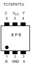
• Package : UF6
• Power-down protection is provided on all inputs and outputsPinout Specifications
|
Characteristics |
Symbol |
Rating |
Unit |
| Power supply voltage |
VCC |
-0.5 to 4.6 |
V |
| DC input voltage |
VIN |
-0.5 to 4.6 |
V |
| DC output voltage |
VOUT |
-0.5 to 4.6 2 |
V |
|
-0.5 to VCC + 0.5 3 |
| Input diode current |
IIK |
-20 |
mA |
| Output diode current |
IOK |
±20 4 |
mA |
| DC output current |
IOUT |
±25 |
mA |
| Power dissipation |
PD |
180 |
mW |
| DC VCC/ground current |
ICC/IGND |
±25 |
mA |
| Storage temperature |
Tstg |
-65~150 |
°C |
Note 1: Exceeding any of the absolute maximum ratings, even briefly, lead to deterioration in IC performance or even destruction. Using continuously under heavy loads (e.g. the application of high temperature/current/voltage and the significant change in temperature, etc.) may cause this product to decrease in the reliability significantly even if the operating conditions (i.e. operating temperature/current/voltage, etc.) are within the absolute maximum ratings and the operating ranges. Please design the appropriate reliability upon reviewing the Toshiba Semiconductor Reliability Handbook ("Handling Precautions"/"Derating Concept and Methods") and individual reliability data (i.e. reliability test report and estimated failure rate, etc).
Note 2: VCC = 0 V
Note 3: High or Low state. IOUT absolute ratiingmust be observed.
Note 4: VOUT < GND, VOUT > VCC
DescriptionThe TC7SP97,98 is a high performance CMOS multiple Function Gate which is guaranteed to operate from 1.2-V to 3.6-V.Designed for use in 1.5 V, 1.8 V, 2.5 V or 3.3 V systems, it achieves high speed operation while maintaining the CMOS low power dissipation.
TC7SP97 is also designed with over voltage tolerant inputs and outputs up to 3.6 V.It independently consists of three circuits for Multiple Function Gate.The output state is determined by seven patterns of 3-inputs.
The user of TC7SP97can choose the functions of Multiplexer, AND, OR,NAND, Schmitt Inverter, and Schmitt Buffer.All inputs are equipped with protection circuits against static discharge.

 TC7SP97 Data Sheet


