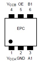
Features: • Operating voltage range:VCCA = 1.1 to 2.7 V (Control portion)VCCB = 1.65 to 3.6 V (Switch portion)• ON-resistance: RON = 8 (max) (VCCB = 2.7 V) RON = 10 (max) (VCCB = 2.3 V)• ESD performance: Machine model ±200 V Human body model ±2000 V• Ultra-small package...
TC7SP3067TU: Features: • Operating voltage range:VCCA = 1.1 to 2.7 V (Control portion)VCCB = 1.65 to 3.6 V (Switch portion)• ON-resistance: RON = 8 (max) (VCCB = 2.7 V) RON = 10 (max) (VCCB = 2.3 V...
SeekIC Buyer Protection PLUS - newly updated for 2013!
268 Transactions
All payment methods are secure and covered by SeekIC Buyer Protection PLUS.
US $.05 - .08 / Piece
Gates (AND / NAND / OR / NOR) 2-Input NAND Gate 5Pin High Speed
Characteristics |
Symbol |
Rating |
Unit |
Power supply voltage (Note 2) |
VCCA |
−0.5 to 4.6 |
V |
VCCB |
−0.5 to 4.6 | ||
Control input voltage (OE (3066)/ OE (3067)) |
VIN |
−0.5 to 4.6 |
V |
Switch input/output voltage |
Vs |
−0.5 to VCCB + 0.5 |
V |
Diode current in the control portion |
IIK |
-25 |
mA |
Diode current in the switch portion |
IIK |
±50 (Note 3) |
mA |
Switch input/output current |
IS |
128 |
mA |
DC VCC/ground current |
ICCA |
±50 |
mA |
ICCB |
±100 | ||
Power dissipation |
PD |
200 |
mW |
Storage temperature |
Tstg |
−65 to 150 |
°C |
Note 1: Exceeding any of the absolute maximum ratings, even briefly, lead to deterioration in IC performance or even
destruction. Using continuously under heavy loads (e.g. the application of high temperature/current/voltage and the significant change in temperature, etc.) may cause this product to decrease in the reliability significantly even if the operating conditions (i.e. operating temperature/current/voltage, etc.) are within the absolute maximum ratings and the operating ranges. Please design the appropriate reliability upon reviewing the Toshiba Semiconductor Reliability Handbook ("Handling Precautions"/"Derating Concept and Methods") and individual reliability data (i.e. reliability test report and estimated failure rate, etc).
Note 2: Do not supply a voltage to the VCCB pin when VCCA is in the OFF state.
Note 3: VS < GND, VS > VCCB
The TC7SP3067TU is high-speed CMOS one-bit analog bus switches with separate power supplies for control and switch portions. In the TC7SP3066, the switch is on when Output Enable (OE) is High. In the TC7SP3067, the switch is on when Output Enable (OE ) is Low.
The TC7SP3067TU support power-down protection by incorporating 3.6-V-torelant control inputs.
The TC7SP3067TU is suitable for applications where the control voltage is lower than the signal line voltage.
All inputs of TC7SP3067TU are equipped with protection circuits against static discharge or transient excess voltage.