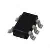
DescriptionThe TC7SL02F is a low voltage operating C2MOS 2-INPUT NOR GATE frabricated with silicon gate C2MOS technology. The feature of TC7SL02F are as follows: (1)high speed: tpd = 10ns at VCC = 3V; (2)low power dissipation: ICC = 1A at Ta = 25; (3)high noise immunity: VNIH = VNIL = 28% Vcc; (4)...
TC7SL02F: DescriptionThe TC7SL02F is a low voltage operating C2MOS 2-INPUT NOR GATE frabricated with silicon gate C2MOS technology. The feature of TC7SL02F are as follows: (1)high speed: tpd = 10ns at VCC = 3...
SeekIC Buyer Protection PLUS - newly updated for 2013!
268 Transactions
All payment methods are secure and covered by SeekIC Buyer Protection PLUS.
US $.05 - .08 / Piece
Gates (AND / NAND / OR / NOR) 2-Input NAND Gate 5Pin High Speed
The TC7SL02F is a low voltage operating C2MOS 2-INPUT NOR GATE frabricated with silicon gate C2MOS technology. The feature of TC7SL02F are as follows: (1)high speed: tpd = 10ns at VCC = 3V; (2)low power dissipation: ICC = 1A at Ta = 25; (3)high noise immunity: VNIH = VNIL = 28% Vcc; (4)symmertrical output impedance: IOH = IOL = 1mA; (5)balanced propagation delays: tpLHtpHL; (6)low voltage operating: VCC(opr.) = 1V~3.6V.
The absolute maximum ratings of the TC7SL02F are: (1)supply voltage range: -0.5~5.0V; (2)DC input voltage: -0.5~Vcc + 0.5V; (3)DC output voltage: -0.5~Vcc + 0.5V; (4)input diode current: ±20mA; (5)output diode current: ±20mA; (6)DC output current: ±12.5mA; (7)DC VCC/Ground current: ±25mA; (8)power dissipation: 200mW; (9)storage temperature: -65~150; (10)lead temperature: 260.
The following is about the electrical characteristics of TC7SL02F: (1)high-level input voltage: 0.75V min; (2)low-level input voltage: 0.25V max; (3)high-level output voltage: 0.9V min and 1.0V typical at VIN = VIH or VIL, IOH = -20A, 1.07V min and 1.23V typical at VIN = VIH or VIL, IOH = -1mA; (4)low-level output voltage: 0.0V typical and 0.1V max at VIN = VIH or VIL, IOH = 20A, 0.23V typical and 0.31V max at VIN = VIH or VIL, IOH = 1mA; (5)input leakage current: ±0.1A max at VIN = VCC or GND; (7)quiescent supply current: 1.0A max at VIN = Vcc or GND.