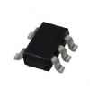
Features: SpecificationsDescription TC7SET04F is a kind of advanced high speed CMOS INVERTER fabricated with silicon gate CMOS technology.It achieves the high speed operation similar to equivalent Bipolar Schotty TTL while maintaining the CMOS low power dissipation.The input threshold levels are c...
TC7SET04F: Features: SpecificationsDescription TC7SET04F is a kind of advanced high speed CMOS INVERTER fabricated with silicon gate CMOS technology.It achieves the high speed operation similar to equivalent B...
SeekIC Buyer Protection PLUS - newly updated for 2013!
268 Transactions
All payment methods are secure and covered by SeekIC Buyer Protection PLUS.
US $.05 - .08 / Piece
Gates (AND / NAND / OR / NOR) 2-Input NAND Gate 5Pin High Speed
TC7SET04F is a kind of advanced high speed CMOS INVERTER fabricated with silicon gate CMOS technology.It achieves the high speed operation similar to equivalent Bipolar Schotty TTL while maintaining the CMOS low power dissipation.The input threshold levels are compatible with TTL output voltage.This device can be used for level converter for interfacing 3 V to 5 V system.An input protection circuit ensures that 0 V to 7 V can be applied to the input pins without regard to the supply voltage.
What comes next is about the maximum ratings of TC7SET04F.The VCC (supply voltage range) is from -0.5 to 7.0 V.The VIN (DC input voltage) is from -0.5 to 7.0 V.The VOUT (DC output voltage) is from -0.5 to VCC+0.5 V.The IOUT (DC output current) is ±25 mA.The ICC (DC VCC/ground current) is ±50 mA.The IIK (input diode current) is -20 mA.The IOK (output diode current) is ±20 mA.The PD (power dissipation) is 200 mW.The Tstg (storage temperature range) is from -65 to 150.The lead temperature (10s) (TL) is 260.Then is about the recommended operating conditions.The VCC (supply voltage) is from 4.5 to 5.5 V.The VIN (input voltage) is from 0 to 5.5 V.The VOUT (output voltage) is from 0 to VCC V.The Topr (operating temperature range) is from -45 to 85.The dt/dv (input rise and fall time) is from 0 to 20 ns/V.
The following is about the DC electrical characteristics of TC7SET04F (Ta=25).The minimum VIH (high-level input voltage) is 2.0 V at VCC=4.5 to 5.5 V.The maximum VIL (low-level input voltage) is 0.8 V at VCC=4.5 to 5.5 V.The maximum 3-state output off-state current (IOZ) is ±0.5A at VIN=VIH or VIL,VOUT=VCC or GND,VCC=5.5 V.The maximum input leakage current (IIN) is ±0.1A at VIN=VCC or GND,VCC=5.5 V.The maximum quiescent supply current (ICC) is 2.0A at VIN=VCC or GND,VCC=5.5 V.The maximum quiescent supply current (ICCT) is 2.0A when per input:VIN=0.5 V or 2.4 V,VCC=5.5 V;other input:VCC or GND.