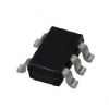
Features: • Operating voltage: VCC = 2~3.6 V• High speed operation: tpd = 0.31 ns (max) @3 V• Low ON-resistance: RON = 5 (typ.) @3 V• ESD performance: Machine model ±200 V Human body model ±2000 V• Power-down protection for inputs. ( OE input only)• Package: ...
TC7SBL384AFU: Features: • Operating voltage: VCC = 2~3.6 V• High speed operation: tpd = 0.31 ns (max) @3 V• Low ON-resistance: RON = 5 (typ.) @3 V• ESD performance: Machine model ±200 V ...
SeekIC Buyer Protection PLUS - newly updated for 2013!
268 Transactions
All payment methods are secure and covered by SeekIC Buyer Protection PLUS.
US $.05 - .08 / Piece
Gates (AND / NAND / OR / NOR) 2-Input NAND Gate 5Pin High Speed
Characteristics | Symbol | Rating | Unit | |
Power supply range | VCC | -0.5~4.6 | V | |
DC input voltage | VIN | -0.5~4.6 | V | |
DC switch voltage | VS | -0.5~Vcc+0.5 | V | |
Input diode current | Control input pin | IIK | -50 | mA |
Switch terminal | ±50 | |||
Continuous channel circuit | IS | 128 | mA | |
Power dissipation | PD | 200 | mW | |
DC VCC/ground current | ICC/IGND | ±100 | mA | |
Storage temperature | Tstg | -65~150 | °C |
Note: Exceeding any of the absolute maximum ratings, even briefly, may lead to deterioration in IC performance or even destruction.
Using continuously under heavy loads (e.g. the application of high temperature/current/voltage and the significant change in temperature, etc.) may cause this product to decrease in the reliability significantly even if the operating conditions (i.e. operating temperature/current/voltage, etc.) are within the absolute maximum ratings and the operating ranges.
Please design the appropriate reliability upon reviewing the Toshiba Semiconductor Reliability Handbook ("Handling Precautions"/"Derating Concept and Methods") and individual reliability data (i.e. reliability test report and estimated failure rate, etc).
The TC7SBL384AFU is a low ON-resistance, high-speed CMOS 1-bit bus switch with low-voltage operation. The low ON-resistance of the switch allows connections to be made with minimal propagation delay.
The TC7SBL384AFU comprises a single-bit low-impedance switch with output-enable ( OE ) input. When OE is low, the switch is on and data can flow from port A to port B, or vice versa. When OE is high, the switch is open and a high-impedance state exists between the two ports.
P-MOS and N-MOS channel blocks also render the TC7SBL384AFU suitable for analog signal transmission.
All inputs of TC7SBL384AFU are equipped with protection circuits to guard against static discharge.