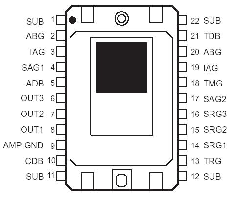
Pinout Specifications
Supply voltage range, VCC: ADB, CDB, TDB (see Note 1). . . . . . . . . . . . . . . . . . . . . 0 V to 15 V
Input voltage range, VI: ABG, IAG, SAG1, SAG2, SRG1, SRG2, SRG3, TRG . . . . . . . 15 V to 15 V
Operating free-air temperature range, TA. . . . . . . . . . . . . . . . . . . . . . . . . . . . . . 10°C to 40°C
Storage temperature range, TSTG . . . . . . . . . . . . . . . . . . . . . . . . . . . . . . . . . . . .30°C to 85°C
Lead temperature 1,6 mm (1/16 in) from case for 10 seconds . . . . . . . . . . . . . . . . . . . . 260°C
DescriptionThe TC271 is a frame-transfer charge-coupled-device (CCD) image sensor with two field memories. It is suitable for use in PAL-video or still-picture photography applications. Its image-sensing area is configured into 580 lines; 576 of these are active and the remaining four are used for dark reference. Each line is configured into 1080 pixels with 1044 active and 36 for dark reference. The TC271 has a standard aspect ratio of 4:3 and a standard 11-mm image-sensing-area diagonal. Its blooming protection, which is an integral part of each pixel, is based on electron-hole recombination and is activated by clocking the antiblooming gate.
One important aspect of the TC271 high-resolution sensor is its ability to simultaneously capture both fields of a TV frame. Its two independently addressable memories allow separate storage of each field and operation in a variety of modes, including CCIR with true interlace, CCIR with pseudointerlace, progressive scan, and nonstandard pseudointerlace with a resolution of 1152 lines.
A unique multiplexer section (see Figure 1) rearranges the horizontal pixels into vertical groups of three and separates and loads the image into the two field memories. The independent addressing of each field memory provides flexibility for different modes of operation. The interdigitated layout of the memories allows each memory to share the same bank of three serial registers and associated charge-detection amplifiers (see Figure 2 and the functional block diagram). Each register and associated amplifier reads out every third column of the image area (see Figure 3). The three amplifiers are optimized dual-source followers that allow the use of off-chip double correlated-clamp sample-and-hold amplifiers for removing KTC noise.
The TC271 is built using TI-proprietary virtual-phase technology, which provides devices with high blue response, low dark current, high photoresponse uniformity, and single-phase clocking. The TC271 is characterized for operation from 10°C to 40°C.

 TC271 Data Sheet


