TC253SPD-B0

Features: *Very Low Noise, High Sensitivity Electronically Variable*High Resolution, 1/3-in Format, Solid State Charge-Coupled Device (CCD) Frame Transfer Image Sensor for Black and White, NTSC, and Computer Applications*340,000 Pixels per Field*Frame Memory*656 (H) 496 (V) Active Pixels in Image ...

product image

TC253SPD-B0 Picture
SeekIC No. : 004513522 Detail

TC253SPD-B0: Features: *Very Low Noise, High Sensitivity Electronically Variable*High Resolution, 1/3-in Format, Solid State Charge-Coupled Device (CCD) Frame Transfer Image Sensor for Black and White, NTSC, and...

floor Price/Ceiling Price

Part Number:
TC253SPD-B0
Supply Ability:
5000

Price Break

  • Qty
  • 1~5000
  • Unit Price
  • Negotiable
  • Processing time
  • 15 Days
Total Cost: $ 0.00

SeekIC Buyer Protection PLUS - newly updated for 2013!

  • Escrow Protection.
  • Guaranteed refunds.
  • Secure payments.
  • Learn more >>

Month Sales

268 Transactions

Rating

evaluate  (4.8 stars)

Upload time: 2025/1/12

Payment Methods

All payment methods are secure and covered by SeekIC Buyer Protection PLUS.

Notice: When you place an order, your payment is made to SeekIC and not to your seller. SeekIC only pays the seller after confirming you have received your order. We will also never share your payment details with your seller.
Product Details

Description


Features:

*Very Low Noise, High Sensitivity
  Electronically Variable
*High Resolution, 1/3-in Format, Solid State
  Charge-Coupled Device (CCD) Frame
  Transfer Image Sensor for Black and White,
  NTSC, and Computer Applications
*340,000 Pixels per Field
*Frame Memory
*656 (H)  496 (V) Active Pixels in Image
  Sensing Area Compatible With Electronic
  Centering
*Multimode Readout Capability
  --- Progressive Scan
  --- Interlace Scan
  --- Line Summing
*Fast Single-Pulse Clear Capability
*Continuous Electronic Exposure Control
  From 1/30 s to 1/5,000 s
*7.4-m Square Pixels
*Advanced Lateral Overflow Drain
*Low Dark Current
*High Photoresponse Uniformity Over a
  Wide Spectral Range
*Solid-State Reliability With No Image
  Burn-In, Resideual Imaging, Image
  Distortion, Image Lag, or Microphonics
*Package With Peltier Cooler


Application

Audio
Automotive
Broadband
Digital Control
Military
Optical Networking
Security
Telephony
Video & Imaging
Wireless


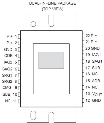
Pinout

  Connection Diagram


Specifications

Supply voltage range, Vss: ADB (see Note 1) . . SUB to SUB + 15 V
Supply voltage range, Vss: ODB . . . . . . . . . . . . . SUB to SUB + 20V
Input voltage range, VI: IAG, SAG, SRG2 . . . . . . . . . . .-8 V to + 8 V
Input voltage range, VI: SRG1 . . . . . . . . . . . . .  . .  . . .-8 V to + 8 V
Input voltage range, VI: CMG . . . . . . . . . . . .  . .  . .. .-5 V to + 15 V
Supply voltage range, Vcool: P+ (see Note2) . . .  . . . . . . .0 V + 3 V
Supply current range, Icool: P+ (see Note2) . . . . . .0 mA to 700 mA
Operating free-air temperature range, TA. . . . . .  . . . .-10 to 45
Storage temperature range, TSTG. . . . . . .  . .  . .  . . . .-30 to 85
Operating case temperature range .. . . . . . . .  . .  . .  .-10 to 55


Description

    The TC253SPD-B0 is a frame-transfer, CCD image sensor designed for use in black and white, NTSC TV, computer, and special-purpose applications requiring high sensitivity, low noise, and small size.

    The TC253SPD-B0 is a new device of the IMPACTRON family of very-low noise, high sensitivity image sensors that multiply charge directly in charge domain before conversion to voltage. The charge carrier multiplication (CCM) is achieved by using a low-noise single-carrier, impact ionization process that occurs during repeated carrier transfers through high-field regions. Applying multiplication pulses to specially designed gates activates the CCM. The amount of multiplication is adjustable depending on the amplitude of the multiplication pulses. The device function resembles the function of image intensifiers implemented in solid state.

    The image-sensing area of the TC253SPD-B0 is configured into 500 lines with 680 pixels in each line. Twenty-four pixels are reserved in each line for dark reference. The blooming protection is based on an advanced lateral overflow drain concept that does not reduce NIR response. The sensor can be operated in the interlaced or progressive scan modes and can capture a full 340,000 pixels in one image field. The frame transfer from the image sensing area to the memory area is accomplished at a very high rate that minimizes image smear. The electronic exposure control is achieved by clearing unwanted charge from the image area using a short positive pulse applied to the antiblooming drain. This marks the beginning of the integration time, which can be arbitrarily shortened from its nominal length. After the charge is integrated and stored in memory, it becomes available for readout in the next cycle. This is accomplished using a unique serial register design that includes special charge multiplication pixels.

    The TC253SPD-B0 sensor is built using TI-proprietary advanced split-gate virtual-phase CCD (SGVPCCD) technology, which provides devices with wide spectral response, high quantum efficiency (QE), low dark current, and high response uniformity. The TC253SPD-B0 sensors are characterized for operation from -10 to 45.


Customers Who Bought This Item Also Bought

Margin,quality,low-cost products with low minimum orders. Secure your online payments with SeekIC Buyer Protection.
Inductors, Coils, Chokes
Power Supplies - Board Mount
Discrete Semiconductor Products
Programmers, Development Systems
View more