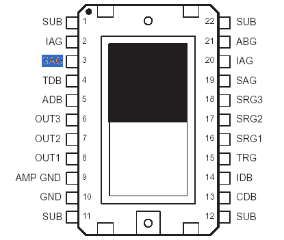
Features: • High-Resolution, Solid-State Image Sensor for NTSC B/W TV Applications
• 11-mm Image-Area Diagonal, Compatible With 2/3" Vidicon Optics
• 754 (H) x 244 (V) Active Elements in Image-Sensing Area
• Low Dark Current
• Electron-Hole Recombination Antiblooming
• Dynamic Range . . . More Than 60 dB
• High Sensitivity
• High Photoresponse Uniformity
• High Blue Response
• Single-Phase Clocking
• Solid-State Reliability With No Image Burn-in, Residual Imaging, Image Distortion, Image Lag, or MicrophonicsPinout Specifications
Supply voltage range, VCC: ADB, CDB, IDB, TDB (see Note 1)........... 0 V to 15 V
Input voltage range, VI: ABG, IAG, SAG, SRG, TRG ........................15 V to 15 V
Operating free-air temperature range, TA .....................................10 to 45
Storage temperature range, TSTG................................................. 30 to 85
Lead temperature 1,6 mm (1/16 inch) from case for 10 seconds ................260
† Stresses beyond those listed under "absolute maximum ratings" may cause permanent damage to the device. These are stress ratings only and functional operation of the device at these or any other conditions beyond those indicated under "recommended operating conditions" is not implied. Exposure to absolute-maximum-rated conditions for extended periods may affect device reliability.
NOTE 1: All voltage values are with respect to the substrate terminal.
DescriptionThe TC241 is a frame-transfer charge-coupled device (CCD) image sensor designed for use in single-chip B/W NTSC TV applications. The device is intended to replace a 2/3-inch vidicon tube in applications requiring small size, high reliability, and low cost.
The image-sensing area of the TC241 is configured into 244 lines with 780 elements in each line. Twenty-four elements are provided in each line for dark reference. The blooming-protection feature of the sensor is based on recombining excess charge with charge of opposite polarity in the substrate. This antiblooming is activated by supplying clocking pulses to the antiblooming gate, which is an integral part of each image- sensing element.
The sensor is designed to operate in an interlace mode, electronically displacing the image-sensing elements by one-half of a vertical line during the charge integration period in alternate fields, effectively increasing the vertical resolution and minimizing aliasing. The device can also be run as a 754 (H) by 244 (V) noninterlaced sensor with significant reduction in the dark signal.
A gated floating-diffusion detection structure with an automatic reset and voltage reference incorporated on-chip converts charge to signal voltage. A low-noise, two-stage, source-follower amplifier buffers the output and provides high output-drive capability.
The TC241 is built using TI-proprietary virtual-phase technology, which provides devices with high blue response, low dark current, high photoresponse uniformity, and single-phase clocking.
The TC241 is characterized for operation from 10 to 45.

 TC241 Data Sheet


