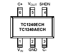
Features: • Charge Pumps in 6-Pin SOT-23A Package
• >99% Typical Voltage Conversion Efficiency
• Voltage Doubling
• Input Voltage Range, TC1240: +2.5V to +4.0V,
TC1240A: +2.5V to +5.5V
• Low Output Resistance, TC1240: 17Ω (Typical)
TC1240A: 12Ω (Typical)
• Only Two External Capacitors Required
• Low Supply Current, TC1240: 180 µA (Typical)
TC1240A: 550 µA (Typical)
• Power-Saving Shutdown Mode (1 µA Maximum)
• Shutdown Input Fully Compatible with 1.8V Logic SystemsApplication• Cellular Phones
• Pagers
• PDAs, Portable Data Loggers
• Battery Powered Devices
• Handheld InstrumentsPinout Specifications
| Typical Active Output Current (mA) | 40 |
| Output Voltage (V) | Vout = 2Vin |
| Typical Quiescent Current (A) | 180 |
| Input Voltage Range (V) | 2.5 to 4.0 |
| Operating Temp. Range (°C) | -45 to 85 |
| Device Description | Inverting or Doubling |
| Typical Active Output Current (mA) |
40 |
| Output Voltage (V) |
Vout = 2Vin |
| Typical Quiescent Current (A) |
180 |
| Input Voltage Range (V) |
2.5 to 4.0 |
| Operating Temp. Range (°C) |
-45 to 85 |
| Device Description |
Inverting or Doubling |
Input Voltage (VIN to GND)
TC1240 .............................................. +4.5V, -0.3V
TC1240A............................................. +5.8V, -0.3V
Output Voltage (VOUT to GND)
TC1240 ........................................ +9.0V, VIN -0.3V
TC1240A..................................... +11.6V, VIN -0.3V
Current at VOUT Pin...........................................50 mA
Short-Circuit Duration: VOUT to GND ............Indefinite
Thermal Resistance ........................................210/W
Power Dissipation (TA = +25)........................600 mW
Operating Temperature Range................-40to +85
Storage Temperature (Unbiased) .........-65to +150
† Stresses above those listed under "Absolute Maximum Ratings" may cause permanent damage to the device. These are stress ratings only and functional operation of the device at these or any other conditions above those indicated in the operation sections of the specifications is not implied. Exposure to Absolute Maximum Rating conditions for extended periods may affect device reliability.
DescriptionThe TC1240 is a doubling CMOS charge-pump voltage converter in a small 6-Pin SOT-23A package. It doubles an input voltage which can range from +2.5V to +4.0V. Conversion efficiency is typically >99%. Internal oscillator frequency is 160kHz for it. The TC1240 has an active high shutdown which limits the current consumption of the device to less than 1A. External component requirement is only two capacitors for standard voltage doubler applications. All other circuitry, including control, oscillator, power MOSFETs are integrated on-chip. Typical supply current is 180A and the device is available in a 6-Pin SOT-23A surface mount package.
The TC1240/TC1240A is a doubling CMOS charge pump voltage converter in a small 6-Pin SOT-23A package. The doubles an input voltage that can range from +2.5V to +4.0V, while the TC1240A doubles an input voltage that can range from +2.5V to +5.5V. Conversion efficiency is typically >99%. Internal oscillator frequency is 160 kHz for both devices. The TC1240 and TC1240A have an active-high shutdown that limits the current consumption of the devices to less than 1 µA.
External component requirement is only two capacitors for standard voltage doubler applications. All other circuitry (including control, oscillator and power MOSFETs) are integrated on-chip. Typical supply current is 180 µA for the TC1240 and 550 µA for the TC1240A. Both devices are available in a 6-Pin SOT- 23A surface mount package.

 TC1240 Data Sheet


