TA75W01FU

Features: · In the linear mode the input common mode voltage range includes ground.· The internally compensated operational amplifier is small package.· Low power dissipation and power drain suitable for battery operation.· Differential input voltage range equal to the power supply voltage.· Large...

product image

TA75W01FU Picture
SeekIC No. : 004512021 Detail

TA75W01FU: Features: · In the linear mode the input common mode voltage range includes ground.· The internally compensated operational amplifier is small package.· Low power dissipation and power drain suitabl...

floor Price/Ceiling Price

Part Number:
TA75W01FU
Supply Ability:
5000

Price Break

  • Qty
  • 1~5000
  • Unit Price
  • Negotiable
  • Processing time
  • 15 Days
Total Cost: $ 0.00

SeekIC Buyer Protection PLUS - newly updated for 2013!

  • Escrow Protection.
  • Guaranteed refunds.
  • Secure payments.
  • Learn more >>

Month Sales

268 Transactions

Rating

evaluate  (4.8 stars)

Upload time: 2025/1/12

Payment Methods

All payment methods are secure and covered by SeekIC Buyer Protection PLUS.

Notice: When you place an order, your payment is made to SeekIC and not to your seller. SeekIC only pays the seller after confirming you have received your order. We will also never share your payment details with your seller.
Product Details

Description


Features:

·  In the linear mode the input common mode voltage range includes ground.
·  The internally compensated operational amplifier is small package.
·  Low power dissipation and power drain suitable for battery operation.
·  Differential input voltage range equal to the power supply voltage.
·  Large output voltage swing : 0VDC to 3.4VDC (VCC = 5VDC)
·  Wide power supply voltage range and single power supply is possible.
·  Single supply 3VDC to 12VDC or dual supplies ± 1.5VDC to ± 6VDC.


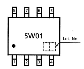
Pinout

  Connection Diagram


Specifications

Characteristic
Symbol
Rating
Unit
Supply voltage

Differential input voltage

Input voltage

Power dissipation

Operating temperature

Storage temperature
VCC, VEE

DVIN

VIN

PD

Topr

Tstg
±6 or 12

±12

−0.3 ~VCC

250

−40~85

−55~125
V

V

V

mW

°C

°C

Note: Using continuously under heavy loads (e.g. the application of high temperature/current/voltage and the significant change in temperature, etc.) may cause this product to decrease in the reliability significantly even if the operating conditions (i.e. operating temperature/current/voltage, etc.) are within the absolute maximum ratings and the operating ranges.
Please design the appropriate reliability upon reviewing the Toshiba Semiconductor Reliability Handbook ("Handling Precautions"/"Derating Concept and Methods") and individual reliability data (i.e. reliability test report and estimated failure rate, etc).


Customers Who Bought This Item Also Bought

Margin,quality,low-cost products with low minimum orders. Secure your online payments with SeekIC Buyer Protection.
Undefined Category
Isolators
Circuit Protection
Prototyping Products
DE1
Programmers, Development Systems
Optoelectronics
View more