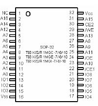
Features: ` Operation voltage. . . . . . T68K1M. . . . . . . . . . . .................2.7V ~ 3.6V T68S1M. . . . . . . . . . . . . . . .. 2.2V ~ 2.7V T68R1M. . . . . . . . . . .................. 1...
T68S1M: Features: ` Operation voltage. . . . . . T68K1M. . . . . . . . . . . .................2.7V ~ 3.6V T68S1M. . . . . . . . . . . . . . . .. 2.2V ~ 2....
SeekIC Buyer Protection PLUS - newly updated for 2013!
268 Transactions
All payment methods are secure and covered by SeekIC Buyer Protection PLUS.
Symbol | Parameter |
Rating |
Unit | |
VCC | Power Supply Voltage (to VSS) |
-0.5 ~ Vcc.max+1V(2) |
V | |
-0.5 ~ Vcc.max+0.3V(3) |
V | |||
VIN/VOUT | Input / Output Voltage |
-0.5 ~ Vcc+0.5V(2) |
V | |
-0.5 ~ Vcc+0.3V(2) |
V | |||
IOUT | Output Current into Outputs (LOW) |
20 |
mA | |
PD | Power Dissipation |
1.0 |
W | |
TSTG | Storage Temperature |
-65 ~ +150 |
||
TSOLDER | Soldering Temperature and Time |
260 OC , 10sec (Lead Only) |
||
TA | Operating Temperature | C-Grade |
0 ~ 70 |
|
E-Grade |
-25 ~ 85 | |||
I-Grade |
-40 ~ 85 |
The T68K1M, T68S1M, and T68R1M device family is a low power and high performance CMOS SRAM organized as 131,072 words by 8 bits. It operates from 2.7V to 3.6V, 2.2V to 2.7V, and 1.65V to 2.2V. Easy memory expansion is provided by an active LOW chip enable 1 (/CE1), active HIGH chp enable 2 (CE2) and active LOW output enable (/OE) and three-state I/O drivers. Four control pins (/CE1, CE2, /OE, and /WE) fully control the operation mode of the T68 K/S/R 1M T68S1M family. An active LOW write enable signal (/WE active low) controls the write/read operation of the memory. When /CE1 and /WE inputs go LOW and CE2 input goes HIGH simultaneously, the T68S1M is in write mode and data on the 8 data pins (IO1~IO8) is written into the memory location specified by the address on address pins (A0~A16). When /CE1 and /OE inputs go LOW and CE2 and /WE input stay in HIGH state, the device is in read mode and data in the specified memory address is driven onto the 8 data pins. The 8 data pins will be in high -impedance state if both /OE and /WE pins are in HIGH (inactive) state. The T68 K/S/R 1M T68S1M family has an automatically power-down feature when the chip is deselected (/CE1 pin HIGH or CE2 pin LOW). The T68 K/S/R 1M device family is available in JEDEC standard 32-pin 450-mil SOP, 32-pin 8mmx20mm plastic TSOP, 32-pin 8mmx13.4mm plastic STSOP, and 36-ball 6mmx8mm BGA package, also for DICE.