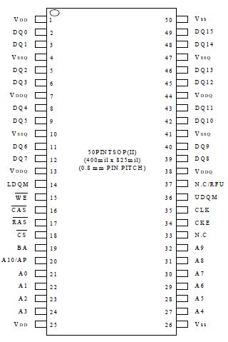
Features: • 3.3V power supply• Clock cycle time : 6 / 7 ns• Dual banks operation• LVTTL compatible with multiplexed address• All inputs are sampled at the positive going edge of system clock• Burst Read Single-bit Write operation• DQM for masking• Au...
T431616C: Features: • 3.3V power supply• Clock cycle time : 6 / 7 ns• Dual banks operation• LVTTL compatible with multiplexed address• All inputs are sampled at the positive goin...
SeekIC Buyer Protection PLUS - newly updated for 2013!
268 Transactions
All payment methods are secure and covered by SeekIC Buyer Protection PLUS.
Parameter |
Symbol |
Value |
Unit |
Voltage on Any Pin Relative To Vss |
VIN,VOUT |
-1.0 to 4.6 |
V |
Supply Voltage Relative To Vss |
VDD,VDDQ |
-1.0 to 4.6 |
V |
Short circuit Output Current |
Iout |
50 |
mA |
Power Dissipation |
PD |
1 |
W |
Operating Temperature |
TOPR |
0 to +70 |
|
Storage Temperature |
Tstg |
-55 to 125 |
Note : Permanent device damage may occur if ABSOLUTE MAXIMUM RATINGS are exceeded.
Functional operation should be restricted to recommended operating condition.
Exposure to higher than recommended voltage for extended periods of time could affect device reliability.
The T431616C is 16,777,216 bits synchronous high data rate Dynamic RAM organized as 2 x 524,288 words by 16 bits , fabricated with high performance CMOS technology . Synchronous design allows precise cycle control with the use of system clock I/O transactions are possible on every clock cycle . Range of operating frequencies , programmable burst length and programmable latencies allow the T431616C to be useful for a variety of high bandwidth , high performance memory system applications.