Features: • High Gain: Typically 35 dB gain across 2.4~2.5 GHz over temperature 0°C to +80°C• High linear output power: >29 dBm P1dB (Exceeding maximum rating of average output power, never measure with CW source! Pulsed single-tone source with <50% duty cycle is recommended.) Me...
SST12LP15: Features: • High Gain: Typically 35 dB gain across 2.4~2.5 GHz over temperature 0°C to +80°C• High linear output power: >29 dBm P1dB (Exceeding maximum rating of average output power,...
SeekIC Buyer Protection PLUS - newly updated for 2013!
268 Transactions
All payment methods are secure and covered by SeekIC Buyer Protection PLUS.
Input power to pins 2 and 3 (PIN) . . . . . . . . . . . . . . . . . . . . . . . . . . . . . . . . . . . . . . . . . . . . . . . . +5 dBm
Average output power (POUT). . . . . . . . . . . . . . . . . . . . . . . . . . . . . . . . . . . . . . . . . . . . . . . . . . +28 dBm
Supply Voltage at pins 5, 12, 14, 16 (VCC) . . . . . . . . . . . . . . . . . . . . . . . . . . . . . . . . . . . .-0.3V to +4.6V
Reference voltage to pins 6 (VREF1) and pin 7 (VREF2) . . . . . . . . . . . . . . . . . . . . . . . . . . . -0.3V to +3.6V
DC supply current (ICC) . . . . . . . . . . . . . . . . . . . . . . . . . . . . . . . . . . . . . . . . . . . . . . . . . . . . . . . .500 mA
Operating Temperature (TA) . . . . . . . . . . . . . . . . . . . . . . . . . . . . . . . . . . . . . . . . . . . . . . .-40 to +85
Storage Temperature (TSTG) . . . . . . . . . . . . . . . . . . . . . . . . . . . . . . . . . . . . . . . . . . . . . -40 to +120
Maximum Junction Temperature (TJ) . . . . . . . . . . . . . . . . . . . . . . . . . . . . . . . . . . . . . . . . . . . . . . +150
Surface Mount Solder Reflow Temperature: . . . . . . . . . . . . . . . . ."with-Pb" units1: 240 for 3 seconds
. . . . . . . . . . . . . . . . . . . . . . . . . . . . . . . . . . . . . . . . . . . . . . . . . . "non-Pb" units: 260 for 3 seconds
1. Certain "with-Pb" package types are capable of 260°C for 3 seconds; please consult the factory for the latest information.
The SST12LP15 is a high-power, high-gain power amplifier based on the highly-reliable InGaP/GaAs HBT technology. The SST12LP15 can be easily configured for high-power, high-efficiency applications with superb power-added efficiency while operating over the 2.4~2.5 GHz frequency band. It typically provides 35 dB gain with 26% poweradded efficiency @ POUT = 24 dBm for 802.11g and 29% power-added efficiency @ POUT = 25 dBm for 802.11b. The SST12LP15 has excellent linearity, typically ~4% added EVM at 23.5 dBm output power which is essential for 54 Mbps 802.11g operation while meeting 802.11g spectrum mask at 24+ dBm. SST12LP15 also has widerange (>25 dB), temperature-stable (~1 dB over 80°C), single- ended/differential power detectors which lower users' cost on power control.
The power amplifier IC also features easy board-level usage along with high-speed power-up/down control. Ultralow reference current (total IREF <2 mA) makes the SST12LP15 controllable by an on/off switching signal directly from the baseband chip. These features coupled with low operating current make the SST12LP15 ideal for the final stage power amplification in battery-powered 802.11g/b WLAN transmitter applications.
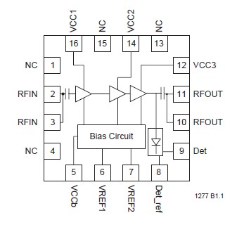
The SST12LP15 is offered in 16-contact VQFN package. See Figure 1 for pin assignments and Table 1 for pin descriptions.