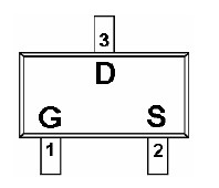
Features: `-20V/-2.4A,RDS(ON)=130mΩ@VGS=- 10V`-20V/-2.9A,RDS(ON)=150mΩ@VGS=- 4.5V`Super high density cell design for extremely low RDS (ON)`Exceptional on-resistance and maximum DC current capability`SOT-323 ( SC70 ) package designApplication·Power Management in Note book·Portable Equi...
SPP1413: Features: `-20V/-2.4A,RDS(ON)=130mΩ@VGS=- 10V`-20V/-2.9A,RDS(ON)=150mΩ@VGS=- 4.5V`Super high density cell design for extremely low RDS (ON)`Exceptional on-resistance and maximum DC curre...
SeekIC Buyer Protection PLUS - newly updated for 2013!
268 Transactions
All payment methods are secure and covered by SeekIC Buyer Protection PLUS.
Parameter | Symbol | Typical | Unit | |
Drain-Source Voltage | VDSS | -20 | V | |
Gate Source Voltage | VGSS | ±12 | V | |
Continuous Drain Current(TJ=150 ) | TA=25 | ID | -2.9 | A |
TA=80 | -2.0 | |||
Pulsed Drain Current | IDM |
-8 | A | |
Continuous Source Current(Diode Conduction) | IS | -1.4 | A | |
Power Dissipation | TA=25 | PD | 0.33 | W |
TA=70 | 0.21 | |||
Operating Junction Temperature |
TJ | -55/150 | ||
Storage Temperature Range | TSTG | -55/150 | ||
Thermal Resistance-Junction to Ambient | RJA | 105 | /W |
The SPP1413 is the P-Channel logic enhancement mode power field effect transistors are produced using high cell density , DMOS trench technology.
This high density process is especially tailored to minimize on-state resistance.
These devices SPP1413 are particularly suited for low voltage application such as cellular phone and notebook computer power management and other battery powered circuits where high-side switching , and low in-line power loss are needed in a very small outline surface mount package.