ApplicationAudio
Automotive
Broadband
Digital Control
Military
Optical Networking
Security
Telephony
Video & Imaging
WirelessPinout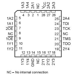
SpecificationsSupply voltage range, VCC . . . . . . . . . . . . . . . . . . . . . . . . . . . . . . . . . . . . . . . . . . . . . . . . . . . . . . . . 0.5 V to 7 V
Input voltage range, VI: except TMS (see Note 1) . . . . . . . . . . . . . . . . . . . . . . . . . . . . . . . . . . . . . . 0.5 V to 7 V
TMS (see Note 1) . . . . . . . . . . . . . . . . . . . . . . . . . . . . . . . . . . . . . . . . . . .0.5 V to 12 V
Voltage range applied to any output in the disabled or power-off state . . . . . . . . . . . . . . . . . . . . 0.5 V to 5.5 V
Voltage range applied to any output in the high state . . . . . . . . . . . . . . . . . . . . . . . . . . . . . . . . . . 0.5 V to VCC
Input clamp current, IIK. . . . . . . . . . . . . . . . . . . . . . . . . . . . . . . . . . . . . . . . . . . . . . . . . . . . . . . . . . . . . . . 30 mA
Current into any output in the low state: SN54BCT8240A (TDO) . . . . . . . . . . . . . . . . . . . . . . . . . . . . . . . . .. 40 mA
SN54BCT8240A (any Y) . . . . . . . . . . . . . . . . . . . . . . . . . . . . . . 96 mA
SN74BCT8240A (TDO) . . . . . . . . . . . . . . . . . . . . . . . . . . . . . . . 48 mA
SN74BCT8240A (any Y) . . . . . . . . . . . . . . . . . . . . . . . . . . . . . 128 mA
Maximum power dissipation at TA = 55 oC (in still air) (see Note 2):DW package . . . . . . . . . . . . . . . . . . . . 1.7 W
NT package . . . . . . . . . . . . . . . . . . . .1.3 W
Storage temperature range, Tstg . . . . . . . . . . . . . . . . . . . . . . . . . . . . . . . . . . . . . . . . . . . . . . . . . .65oC to 150o C
DescriptionThe 'BCT8240A scan test devices with octal buffers are members of the Texas Instruments SCOPE(TM) testability integrated-circuit family. This family of devices SN74BCT8240A supports IEEE Standard 1149.1-1990 boundary scan to facilitate testing of complex circuit-board assemblies. Scan access to the test circuitry is accomplished via the 4-wire test access port (TAP) interface.
In the normal mode, these devices SN74BCT8240A are functionally equivalent to the 'F240 and 'BCT240 octal buffers. The test circuitry can be activated by the TAP to take snapshot samples of the data appearing at the device terminals or to perform a self test on the boundary-test cells. Activating the TAP in normal mode does not affect the functional operation of the SCOPE(TM) octal buffers. In the test mode, the normal operation of the SCOPE(TM) octal buffers is inhibited and the test circuitry is enabled to observe and control the I/O boundary of the device. When enabled, the test circuitry can perform boundary-scan test operations, as described in IEEE Standard 1149.1-1990.
Four dedicated test terminals control the operation of the test circuitry: test data input (TDI), test data output (TDO), test mode select (TMS), and test clock (TCK). Additionally, the test circuitry performs other testing functions such as parallel-signature analysis (PSA) on data inputs and pseudo-random pattern generation (PRPG) from data outputs. All testing and scan operations are synchronized to the TAP interface. The SN54BCT8240A is characterized for operation over the full military temperature range of 55°C to 125°C. The SN74BCT8240A is characterized for operation from 0°C to 70°C.

 SN74BCT8240A Data Sheet