SN74AHC1G08

Features: Operating Range of 2 V to 5.5 VMax tpd of 7 ns at 5 VLow Power Consumption, 10-µA Max ICC±8-mA Output Drive at 5 VSchmitt-Trigger Action at All Inputs Makes the Circuit Tolerant for Slower Input Rise and Fall TimeLatch-Up Performance Exceeds 250 mA Per JESD 17ESD Protection Exceeds...

product image

SN74AHC1G08 Picture
SeekIC No. : 004497977 Detail

SN74AHC1G08: Features: Operating Range of 2 V to 5.5 VMax tpd of 7 ns at 5 VLow Power Consumption, 10-µA Max ICC±8-mA Output Drive at 5 VSchmitt-Trigger Action at All Inputs Makes the Circuit Tolerant for ...

floor Price/Ceiling Price

Part Number:
SN74AHC1G08
Supply Ability:
5000

Price Break

  • Qty
  • 1~5000
  • Unit Price
  • Negotiable
  • Processing time
  • 15 Days
Total Cost: $ 0.00

SeekIC Buyer Protection PLUS - newly updated for 2013!

  • Escrow Protection.
  • Guaranteed refunds.
  • Secure payments.
  • Learn more >>

Month Sales

268 Transactions

Rating

evaluate  (4.8 stars)

Upload time: 2025/1/8

Payment Methods

All payment methods are secure and covered by SeekIC Buyer Protection PLUS.

Notice: When you place an order, your payment is made to SeekIC and not to your seller. SeekIC only pays the seller after confirming you have received your order. We will also never share your payment details with your seller.
Product Details

Description


Features:

Operating Range of 2 V to 5.5 V
Max tpd of 7 ns at 5 V
Low Power Consumption, 10-µA Max ICC
±8-mA Output Drive at 5 V
Schmitt-Trigger Action at All Inputs Makes the Circuit Tolerant for Slower Input Rise and Fall Time
Latch-Up Performance Exceeds 250 mA Per JESD 17
ESD Protection Exceeds JESD 22
  −  2000-V Human-Body Model (A114-A)
  −  200-V Machine Model (A115-A)
  −  1000-V Charged-Device Model (C101)


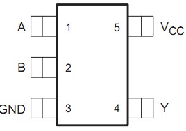
Pinout

  Connection Diagram


Specifications

Supply voltage range, VCC   . . . . . . . . . . . . . . . . . . . . . . . . . −0.5 V to 7 V
Input voltage range, VI (see Note 1)   . . . . . . . . . . . . . . . . . −0.5 V to 7 V
Output voltage range, VO (see Note 1)   . . . . . . . . .−0.5 V to VCC + 0.5 V
Input clamp current, IIK (VI < 0)   . . . . . . . . . . . . . . . . . . . . . . . . . −20 mA
Output clamp current, IOK (VO < 0 or VO > VCC)  . . . . . . . . . . . . . ±20 mA
Continuous output current, IO (VO = 0 to VCC)  . . . . . . . . . . . . . . ±25 mA
Continuous current through VCC or GND  . . . . . . . . . . . . . . . . . . . ±50 mA
Package thermal impedance, JA (see Note 2): DBV package   .  206°C/W
                                                                           DCK package   . 252°C/W
                                                                            DRL package   . 142°C/W
Storage temperature range, Tstg  . . . . . . . . . . . . . . . . . . −65°C to 150°C
† Stresses beyond those listed under "absolute maximum ratings" may cause permanent damage to the device. These are stress ratings only, and functional operation of the device at these or any other conditions beyond those indicated under "recommended operating conditions" is not implied. Exposure to absolute-maximum-rated conditions for extended periods may affect device reliability.
NOTES: 1. The input and output voltage ratings may be exceeded if the input and output current ratings are observed.
             2. The package thermal impedance is calculated in accordance with JESD 51-7.


Description

The SN74AHC1G08 is a single 2-input positive-AND gate. The device performs the Boolean function Y = A • B or Y = AB in positive logic.


Customers Who Bought This Item Also Bought

Margin,quality,low-cost products with low minimum orders. Secure your online payments with SeekIC Buyer Protection.
Computers, Office - Components, Accessories
Optical Inspection Equipment
Audio Products
Optoelectronics
Prototyping Products
DE1
Sensors, Transducers
View more