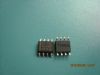
DescriptionThe SN65C3243DR is one of the SN65C3243 series.The SN65C3243DR consists of three line drivers, five line receivers, and a dual charge-pump circuit with ±15-kV ESD protection pin-to-pin (serial-port connection pins, including GND). SN65C3243DR provide the electrical interface between an asynchronous communication controller and the serial-port connector. The charge pump and four small external capacitors allow operation from a single 3-V to 5.5-V supply. In addition, these devices include an always-active noninverting output (ROUT2B), which allows applications using the ring indicator to transmit data while the devices are powered down. The devices operate at data signaling rates up to 1 Mbit/s and an increased slew-rate range of 24 V/µs to 150 V/µs.
Features of the SN65C3243DR are:(1)Operate With 3-V to 5.5-V VCC Supply; (2)Always-Active Noninverting Receiver Output (ROUT2B); (3)Low Standby Current . . . 1 A Typical; (4)External Capacitors . . . 4 * 0.1 F; (5)Accept 5-V Logic Input With 3.3-V Supply; (6)Inter-Operable With SN65C3238, SN75C3238; (7)Support Operation From 250 kbit/s to 1 Mbit/s; (8)RS-232 Bus-Pin ESD Protection Exceeds ±15-kV Using Huma-Body Model (HBM); (9)Latch-Up Performance Exceeds 100 mA Per JESD 78, Class II; (10)Applications: Battery-Powered Systems, PDAs,Notebooks, Laptops, Palmtop PCs, and Hand-Held Equipment.
The absolute maximum ratings of the SN65C3243DR can be summarized as:(1)Supply voltage range, VCC (see Note 1) : -0.3 V to 6 V; (2)Positive output supply voltage range, V+ (see Note 1):-0.3 V to 7 V; (3)Negative output supply voltage range, V- (see Note 1): 0.3 V to -7 V; (4)Supply voltage difference, V+ - V- (see Note 1) 13 V; (5)Input voltage range, VI: Drivers, EN, PWRDOWN:-0.3 V to 6 V;Receivers :-25 V to 25 V; (6)Output voltage range, VO:Drivers -13.2 V to 13.2 V; (7)Receivers:-0.3 V to VCC + 0.3 V; (8)Package thermal impedance, JA (see Notes 2 and 3): DB package 70°C/W;DW package 58°C/W;PW package 83 °C/W; (9)Operating virtual junction temperature, TJ:150°C ; (10)Storage temperature range, Tstg:-65°C to 150°C.
The electrical characteristics(Ta=25) of the SN65C3243DR can be summarized as:(1)VOH:5V MIN 5.4V TYP; (2)IIL:±0.01A TYP ±1A MAX; (3)ro:300 MIN 10M TYPIf you want to know more information such as the electrical characteristics about SN65C3243DR, please download the datasheet in www.seekdatasheet.com .

 SN65C3243DR Data Sheet