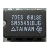
Pinout SpecificationsSupply voltage, VCC+(see Note 3). . . . . . . . . . . . . . . . . . . . . . . . . . . . . . . . . . . . 7 V
Supply voltage, VCC . . . . . . . . . . . . . . . . . . . . . . . . . . . . . . . . . . . . . . . . . . . ..7 V
Differential input voltage, VID (see Note 4) . . . . . . . . . . . . . . . . . . . . . . . . . . ....±6 V
Common-mode input voltage, VIC (see Note 5) . . . . . . . . . . . . . . . . . . . . . . . . ±5 V
Strobe input voltage. . . . . . . . . . . . . . . . . . . . . . . . . . . . . . . . . . . . . . . . . . . . .. 5.5 V
Continuous total dissipation . . . . . . . . . . . . . . . . . . . . . See Dissipation Rating Table
Storage temperature range, Tstg . . . . . . . . . . . . . . . . . . . . . . ..... 65°C to 150°C
Case temperature for 60 seconds, Tc: FK package. . . . . . . . . . . . . . . . . ....... 260°C
Lead temperature 1,6 mm (1/16 inch) from case for 60 seconds: J package ...300°C
Lead temperature 1,6 mm (1/16 inch) from case for 10 seconds: D, N, or W package ...260°C
DescriptionSN55107A is TTL-compatible, high-speed line receivers. Each is a monolithic dual circuit featuring two independent channels. SN55107A is designed for general use, as well as for such specific applications as data comparators and balanced, unbalanced, and party-line transmis-sion systems. These devices are unilaterally interchangeable with and are replacements for the SN55107, SN75107, and SN75108, but offer diode-clamped strobe inputs to simplify circuit design.
The essential difference between the A and B versions can be seen in the schematics. Input-protection diodes of SN55107A are in series with the collectors of the differential-input transistors of the B versions. SN55107A is useful in certain party-line systems that have multiple VCC+ power supplies and can be operated with some of the VCC+ supplies turned off. In such a system, if a supply is turned off and allowed to go to ground, the equivalent input circuit connected to that supply would be as follows:
This would be a problem in specific systems that might have the transmission lines biased to some potential greater than 1.4 V.
The SN55107A is characterized for operation over the full military temperature range of 55°C to 125°C. The SN75107A, SN75107B, and SN75108A are characterized for operation from 0°C to 70°C.

 SN55107A Data Sheet


