Features: · Word-organized programmable nonvolatile memory in n-channel floating-gate technology (E2PROM)
· 256 ´ 8-bit organization
· Supply voltage 5 V
· Serial 2-line bus for data input and output (I2C Bus)
· Reprogramming mode, 10 ms erase / write cycle
· Reprogramming by means of on-chip control (without external control)
· Check for end of programming process
· Programming protect mode
· Data retention > 10 years
· More than 104 reprogramming cycles per addressPinout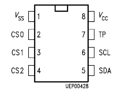 Specifications
| Parameter |
Symbol |
Limit Values |
Unit |
| min. |
max. |
| Supply voltage |
VCC |
0.3 |
6 |
V |
| Input voltage |
VI |
0.3 |
6 |
V |
| Power dissipation |
PD |
|
130 |
mW |
| Storage temperature |
Tstg |
40 |
125 |
°C |
Thermal resistance
(system-air) |
Rth SA |
|
100 |
K/W |
| Junction temperature |
T |
|
85 |
°C |
| Operating Range |
| Supply voltages |
VCC |
4.75 |
5.25 |
V |
| Ambient temperature |
TA |
0 |
70 |
°C |
DescriptionThe I
2C Bus SDA 3526-5 is a bidirectional 2-line bus for the transfer of data between various integrated circuits. SDA 3526-5 consists of a serial data line SDA and a serial clock line SCL. The data line requires an external pull-up resistor to VCC (open drain output stage).
The possible operational states of the I
2C Bus SDA 3526-5 are shown in figure 1. In the quiescent state, both lines SDA and SCL are high, i.e. the output stage of the data line is disabled. As long a SCL remains "1", information changes on the data bus SDA 3526-5 indicate the start or the end of data transfer between two components.
The transition on SDA SDA 3526-5 from "1" to "0" is a start condition, the transition from "0" to "1" is a stop condition. During a data transfer the information on the data bus will only change while the clock line SCL is "0". The information of SDA 3526-5 on SDA is valid as long as SCL is "1".
In conjunction with an I
2C Bus SDA 3526-5 system, the memory component can operate as a receiver and as a transmitter (slave receiver or slave transmitter). Between a start and stop condition, information is always transmitted in byte-organized form. Between the falling edge of the eighth clock pulse and a ninth acknowledge clock pulse, the memory component sets the SDA-line to low as a confirmation of reception, if the SDA 3526-5 select conditions have been met. During the output of data, the data output of the SDA 3526-5 is high in impedance during the ninth clock pulse (acknowledge master).
The signal timing required for the operation of the I2C Bus SDA 3526-5 is summarized in figure 2.

 SDA 3526-5 Data Sheet


