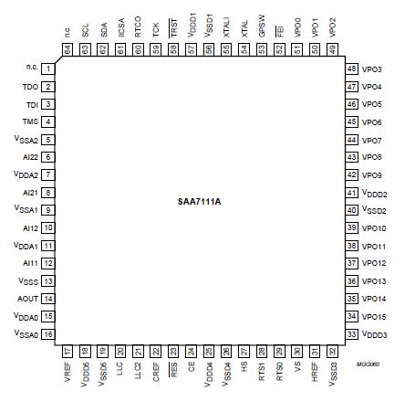
Features: ` Four analog inputs, internal analog source selectors, e.g. 4 * CVBS or 2 * Y/C or (1 * Y/C and 2 * CVBS)
` Two analog preprocessing channels
` Fully programmable static gain for the main channels or automatic gain control for the selected CVBS or Y/C channel
` Switchable white peak control
` Two built-in analog anti-aliasing filters
` Two 8-bit video CMOS analog-to-digital converters
` On-chip clock generator
` Line-locked system clock frequencies
` Digital PLL for horizontal-sync processing and clock generation
` Requires only one crystal (24.576 MHz) for all standards
` Horizontal and vertical sync detection
` Automatic detection of 50 and 60 Hz field frequency, and automatic switching between PAL and NTSC standards
` Luminance and chrominance signal processing for PAL BGHI, PAL N, PAL M, NTSC M, NTSC N, NTSC 4.43, NTSC-Japan and SECAM
` User programmable luminance peaking or aperture correction
` Cross-colour reduction for NTSC by chrominance comb filtering
` PAL delay line for correcting PAL phase errors
` Real time status information output (RTCO)
` Brightness Contrast Saturation (BCS) control on-chip
` The YUV (CCIR-601) bus supports a data rate of:
864 * fH = 13.5 MHz for 625 line sources
858 * fH = 13.5 MHz for 525 line sources.
` Data output streams for 16, 12 or 8-bit width with the following formats:
YUV 4 : 1 : 1 (12-bit)
YUV 4 : 2 : 2 (16-bit)
YUV 4 : 2 : 2 (CCIR-656) (8-bit)
RGB (5, 6, and 5) (16-bit) with dither
RGB (8, 8, and 8) (24-bit) with special application.
` Odd/even field identification by a non interlace CVBS input signal
` Fix level for RGB output format during horizontal blanking
` 720 active samples per line on the YUV bus
` One user programmable general purpose switch on an output pin
` Built-in line-21 text slicer
` A 27 MHz Vertical Blanking Interval (VBI) data bypass programmable by I2C-bus for INTERCAST applications
` Power-on control
` Two via I2C-bus switchable outputs for the digitized CVBS or Y/C input signals AD1 (7 to 0) and AD2 (7 to 0)
` Chip enable function (reset for the clock generator and power save mode up from chip version 3)
` Compatible with memory-based features (line-locked clock)
` Boundary scan test circuit complies with the'IEEE Std. 1149.1 - 1990' (ID-Code = 0 F111 02 B)
` I2C-bus controlled (full read-back ability by an external controller)
` Low power (<0.5 W), low voltage (3.3 V), small package (LQFP64)
` 5 V tolerant digital I/O ports.
Application· Desktop/Notebook (PCMCIA) video
· Multimedia
· Digital television
· Image processing
· Video phone
· Intercast.Pinout Specifications
| SYMBOL |
PARAMETER |
CONDITIONS |
MIN. |
MAX. |
UNIT |
| VDDD |
digital supply voltage |
|
-0.5 |
+4.6 |
V |
| VDDA |
analog supply voltage |
|
-0.5 |
+4.6 |
V |
| Vi(A) |
input voltage at analog inputs |
|
-0.5 |
VDDA + 0.5
(4.6 max.) |
V |
| Vo(A) |
output voltage at analog output |
|
-0.5 |
VDDA + 0.5 |
V |
| Vi(D) |
input voltage at digital inputs and outputs |
outputs in 3-state |
-0.5 |
+5.5 |
V |
| Vo(D) |
output voltage at digital outputs |
outputs active |
-0.5 |
VDDD + 0.5 |
V |
| VSS |
voltage difference between VSSAall and VSSall |
|
- |
100 |
mV |
| Tstg |
storage temperature |
|
-65 |
+150 |
°C |
| Tamb |
operating ambient temperature |
|
0 |
70 |
°C |
| Tamb(bias) |
operating ambient temperature under bias |
|
-10 |
+80 |
°C |
| Vesd |
electrostatic discharge all pins |
note 1 |
-2000 |
+2000 |
V |
Note
1. Human body model: equivalent to discharging a 100 pF capacitor through a 1.5 k resistor.DescriptionThe Enhanced Video Input Processor (EVIP)SAA7111A is a combination of a two-channel analog preprocessing circuit including source selection, anti-aliasing filter and ADC, an automatic clamp and gain control, a Clock Generation Circuit (CGC), a digital multi-standard decoder (PAL BGHI, PAL M, PAL N, NTSC M, NTSC-Japan NTSC N and SECAM), a brightness/contrast/saturation control circuit, a colour space matrix (see Fig.1) and a 27 MHz VBI-data bypass.
The pure 3.3 V CMOS circuit SAA7111A, analog front-end and digital video decoder, is a highly integrated circuit for desktop video applications. The decoder is based on the principle of line-locked clock decoding and is able to decode the colour of PAL, SECAM and NTSC signals into CCIR-601 compatible colour component values. The SAA7111A accepts as analog inputs CVBS or S-video (Y/C) from TV or VTR sources. The circuit is I2C-bus controlled. The SAA7111A then supports several text features as Line 21 data slicing and a high-speed VBI data bypass for Intercast.

 SAA7111A Data Sheet


