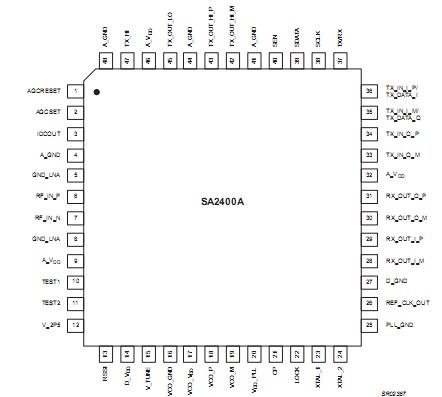
Features: • A 79 dB adjustable gain range direct conversion zero IF receiverwith 3 µs (typical) Tx to Rx switching time, and comprising the following:
Front-end LNA with two internal gain states
A fast on-chip closed loop composite RF and IF AGC with zoomed analog RSSI output and 8 µs settling time
Quadrature downconverters from 2.45 GHz RF directly to zero IF
On-chip fast baseband DC cancellation with automatically stepped bandwidths of 10 MHz, 1 MHz, 100 kHz, and 10 kHz,settling within 813 µs for a DC error of 10% that decays to 1%.
Fully integrated channel filters, appropriate for 11 Msymbols/s QPSK modulation RF bandwidth.
• An I/Q upconverter from baseband directly to 2.45 GHz, with+8 dBm output power, 40 dBc typical carrier leakage (calibrated) and 3 µs (typical) Rx to Tx switching time, and comprising the following:
Wide band IQ modulator producing better than 14% EVM for 11 Msymbols/s QPSK modulation
Integrated reconstruction and spectral shaping filters at I and Qmodulation input that is driven by an external D/A. High common mode rejection to input ground bounce.
FIR-DACs for digital I/Q input feeding the analog signal path and including additional filtering for spectral shaping.
2.45 GHz power amplifier driver with +8 dBm maximum output,15 dB adjustable gain in 1 dB steps and a second switched output at 1.5 dBm power level with similar gain adjustments that are set by a separate register.
Completely on-chip calibration for Carrier Leakage compensation.
Internal power ramping with 2 µs delay and 0.5 µs ramp-up time.
• A fractional-N frequency synthesizer with on-chip VCO and XO
• A 3-wire bus for control of most blocks
• An additional high speed 3-wire bus for full control of Rx-Gain and DC-offset compensation parameters with 44Mbits/s.
• Fast Tx-Rx switching based on a single digital input pin.
• Reference currents and voltage for supply of Baseband Processor and PA-chip.
ApplicationIEEE 802.11 and 802.11b radios
Supports DSSS and CCK modulation
Supports data rates: 1, 2, 5.5, and 11 Mbps
2.45 GHz ISM band wireless communication devicesPinout Specifications
|
Symbol |
Parameter |
Min |
Max |
Unit |
|
Tstg |
Storage temperature |
55 |
+150 |
|
|
VDD |
Supply voltage |
0.5 |
+3.85 |
V |
|
|
Voltage applied to inputs |
0.5 |
VDD+0.5 |
V |
|
|
Short circuit duration, to GND or VDD |
|
1 |
second |
DescriptionThe SA2400A is a fully integrated single IC RF transceiver designed for 2.45 GHz wireless LAN (WLAN) applications. It is a direct conversion radio architecture that is fabricated on an advanced 30 GHz fT BiCMOS process. The SA2400A combines a receiver,transmitter, and LO generation into a single IC. The SA2400A receiver consists of a low-noise amplifier, down-conversion mixers, fully integrated channel filters, and an Automatic Gain Control (AGC) with an on-chip closed loop. The transmitter contains power ramping,filters, up-conversion, and pre-drivers. The LO generation is formed
by an entirely on-chip VCO and a fractional-N synthesizer.
Typical system performance parameters for the SA2400A receiver are 93 dB gain, 7.5 dB noise figure, input-referred third-order intercept point(IIP3) of +1 dBm, AGC settling time of 8 µs, and Tx-to-Rx switching time of 3 µs. The transmitter typical system performance parameters are an output power range from 7 dBm to +8 dBm in 1 dB steps,40 dBc carrier leakage after calibration, 22 dB sideband suppression, in-band common mode rejection of 30 dB, and Rx-to-Tx switching time of 3 µs.

 SA2400A Data Sheet


