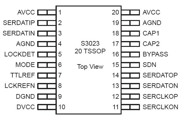
Features: • Complies with Bellcore and ITU-T specifications for jitter tolerance, jitter transfer and jitter generation• On-chip high frequency PLL with internal loop filter for clock recovery• Supports clock recovery for OC-12/STM-(622.08 Mbit/s) or OC-3/STM-1 (155.52 Mbit/s) NR...
S3023: Features: • Complies with Bellcore and ITU-T specifications for jitter tolerance, jitter transfer and jitter generation• On-chip high frequency PLL with internal loop filter for clock re...
SeekIC Buyer Protection PLUS - newly updated for 2013!
268 Transactions
All payment methods are secure and covered by SeekIC Buyer Protection PLUS.
Parameter | Min | Typ | Max | Units |
Storage Temperature | -65 | 150 | °C | |
Voltage on VCC with Respect to GND | -0.5 | +7.0 | V | |
Voltage on any LVTTL Input Pin | -0.5 | VCC | V | |
Voltage on any LVPECL Input Pin | V CC 2.0 |
VCC | V | |
LVTTL Output Sink Current | 20 | mA | ||
LVTTL Output Source Current | 10 | mA | ||
High Speed LVPECL Output Source Current | 50 | mA | ||
ESD Sensitivity 1 | Under 500 | V |
The function of the S3023 clock recovery unit is to derive high speed timing signals for SONET/SDHbased equipment. The S3023 is implemented using AMCC's proven Phase Locked Loop (PLL) technology.
The S3023 receives either an OC-12/STM-4 or OC-3/ STM-1 scrambled NRZ signal and recovers the clock from the data. The chip outputs a differential LVPECL bit clock and retimed data. Figure 1 shows a typical network application.
The S3023 utilizes an on-chip PLL which consists of a phase detector, a loop filter, and a voltage controlled oscillator (VCO). The phase detector compares the phase relationship between the VCO output and the reference frequency. A loop filter of S3023 converts the phase detector output into a smooth DC voltage, and the DC voltage is input to the VCO whose frequency is varied by this voltage. A block diagram is shown in Figure 2.