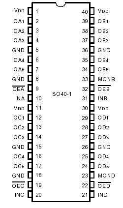
Features: • 20 output, low skew clock signal buffer• High drive FCT-type outputs• Reduced swing TTL outputs for low noise• Input hysteresis for better noise margin• Monitor output• Guaranteed low skew 0.5ns output skew 0.7ns pulse skew 1ns part-to-part skew̶...
QS5820T: Features: • 20 output, low skew clock signal buffer• High drive FCT-type outputs• Reduced swing TTL outputs for low noise• Input hysteresis for better noise margin• Mon...
SeekIC Buyer Protection PLUS - newly updated for 2013!
268 Transactions
All payment methods are secure and covered by SeekIC Buyer Protection PLUS.
Rating |
Symbol |
Max |
unit |
Supply Voltage Range |
VTERM(2) |
0.5 to +4.6
|
V |
Input Voltage Range |
VI (2)
|
0.5 to +5.5 |
V |
Voltage range applied to any output in the high or low state |
VO(2) |
0.5 to VDD + 0.5
|
V |
Input clamp current |
IIK (VI < 0)
|
50 |
mA |
Terminal Voltage with Respect to GND (inputs VIH 2.5, VIL 2.5) |
IOK (VO < 0 or VO > VDD) |
-50
|
mA |
Continuous Output Current |
IRES |
±100 |
mA |
Maximum Power Dissipation |
VDD or GND |
65 to +150 |
mA |
Storage Temperature Range |
TSTG |
150 |
°C |
NOTES:
1. Stresses greater than those listed under ABSOLUTE MAXIMUM RATINGS may cause permanent damage to the device. This is a stress rating only and functional operation of the device at these or any other conditions above those indicated in the operational sections of this specification is not implied. Exposure to absolute maximum rating conditions for extended periods may affect reliability.
2. VDD Terminals.
3. All terminals except VDD.
The QS5820T clock driver/buffer circuits can be used for clock distribution schemes where low skew, high speed, and small footprint are primary concerns. The QS5820T offers four banks of five non-inverting outputs. Designed in IDT's proprietary QCMOS process, this device provides low propagation delay buffering with on-chip skew of 0.5ns for same-transition, same-bank signals. The QS5820T provides major skew advantages over octal type devices where total part-to-part skew (tSK( of >1ns is unacceptable. Furthermore, board area consumed by the QVSOP package is almost one-third that of the typical SOIC package offered for octal devices. This clock buffer product is designed for use high performance workstation, multi-board computing and telecommunications systems. The QS5820T is available in the 40-pin QVSOP package which offers the world's smallest logic footprint.