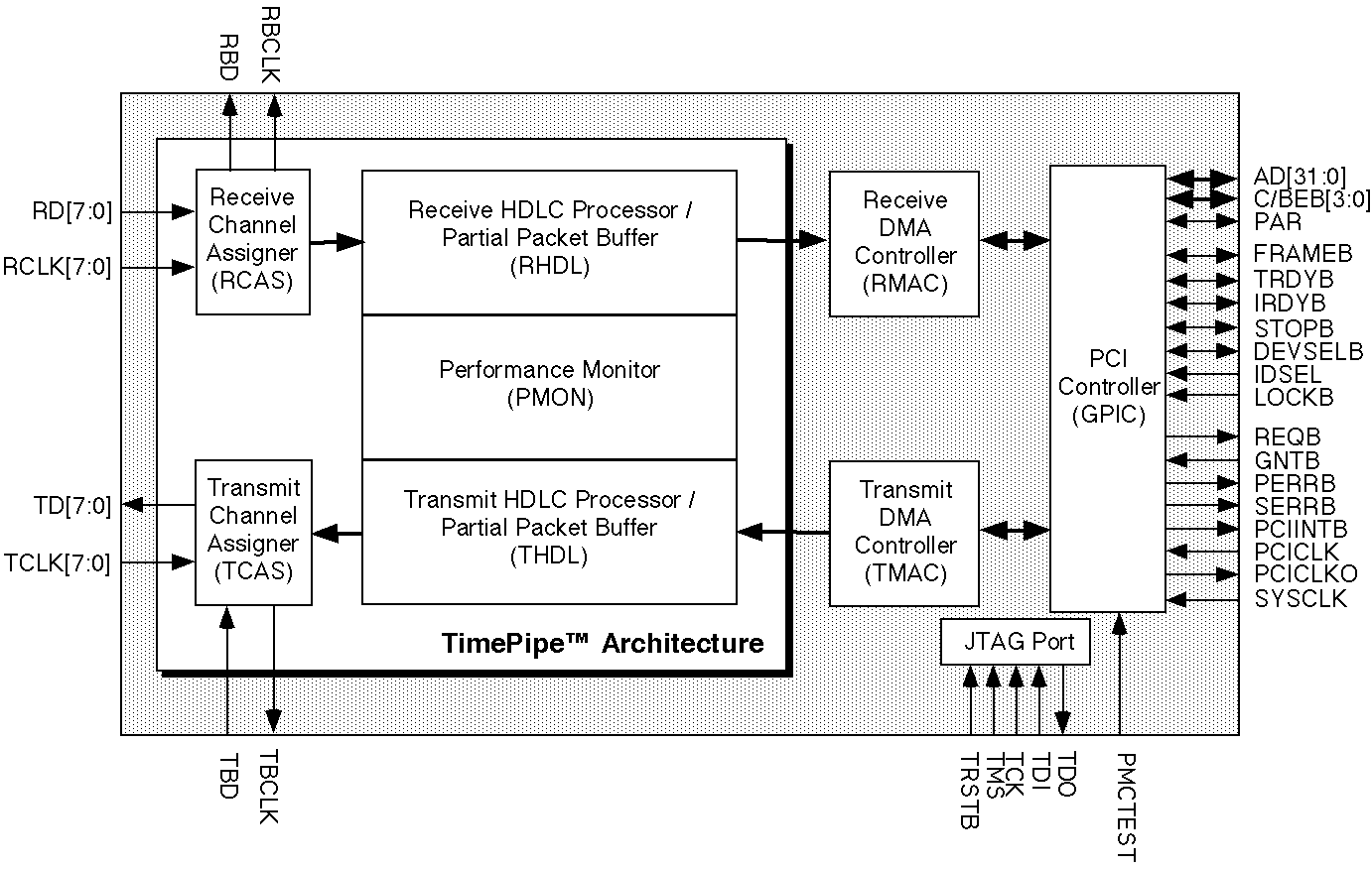
Features: ·Single-chip Peripheral Component Interconnect (PCI) Bus multi-channel HDLC controller.
·Supports up to 128 bi-directional HDLC channels assigned to a maximum of 8 channelised T1 or E1 links. The number of time-slots assigned to an HDLC channel is programmable from 1 to 24 (for T1) and from 1 to 31 (for E1).
·Supports up to 8 bi-directional HDLC channels each assigned to an unchannelised arbitrary rate link; subject to a maximum aggregate link clock rate of 64 MHz in each direction. Channels assigned to links 0 to 2 can have a clock rate of up 52 MHz when SYSCLK is at 33 MHz. Channels assigned to links 3 to 7 can have a clock rate of up to 10 MHz.
·Supports up to two bi-directional HDLC Channels each assigned to an unchannelised arbitrary rate link of up to 52 MHz when SYSCLK is at 33 MHz.
·Supports a mix of up to 8 channelised and unchannelised links; subject to the constraint of a maximum of 128 channels and a maximum aggregate link clock rate of 64 MHz in each direction.
·For each channel, the HDLC receiver performs flag sequence detection, bit de-stuffing, and frame check sequence validation. The receiver supports the validation of both CRC-CCITT and CRC-32 frame check sequences. The receiver also checks for packet abort sequences, octet aligned packet length and for minimum and maximum packet length.
·Alternatively, for each channel, the receiver supports a transparent mode where each octet is transferred transparently to host memory. For channelised links, the octets are aligned with the receive time-slots.
·For each channel, time-slots are selectable to be in 56 kbits/s format or 64 kbits/s clear channel format.
·For each channel, the HDLC transmitter performs flag sequence generation, bit stuffing, and, optionally, frame check sequence generation. The transmitter supports the generation of both CRC-CCITT and CRC-32 frame check sequences. The transmitter also aborts packets under the direction of the host or automatically when the channel underflows.
·Supports two levels of non-preemptive packet priority on each transmit channel. Low priority packets will not begin transmission until all high priority packets are transmitted.
·Alternatively, for each channel, the transmitter supports a transparent mode where each octet is inserted transparently from host memory. For channelised links, the octets are aligned with the transmit time-slots.
·Directly supports a 32-bit, 33 MHz PCI 2.1 interface for configuration, monitoring and transfer of packet data, with an on-chip DMA controller with scatter/gather capabilities.
·Provides 8 kbytes of on-chip memory for partial packet buffering in each direction. This memory can be configured to support a variety of different channel configurations from a single channel with 8 kbytes of buffering to 128 channels, each with a minimum of 48 bytes of buffering.
·Supports PCI burst sizes of up to 128 bytes for transfers of packet data.
·Pin compatible with PM7364 (FREEDM-32) device.
·Provides a standard 5 signal P1149.1 JTAG test port for boundary scan board test purposes.
·Supports 3.3 and 5 Volt PCI signaling environments.
·Low power CMOS technology.
·256 pin enhanced ball grid array (SBGA) or 272 pin plastic ball grid array (PBGA) packages (27 mm X 27 mm).
Application· IETF PPP interfaces for routers
· Frame Relay interfaces for ATM or Frame Relay switches and multiplexors
· FUNI or Frame Relay service inter-working interfaces for ATM switches and multiplexors.
· D-channel processing in ISDN terminals and switches.
· Internet/Intranet access equipment.
· Packet-based DSLAM equipment.Pinout Specifications
Ambient Temperature under Bias
Storage Temperature
Supply Voltage (VDD)
Bias Voltage (VBIAS)
Voltage on Any Pin
Static Discharge Voltage
Latch-Up Current
DC Input Current
Lead Temperature
Absolute Maximum Junction Temperature |
-40°C to +85°C
-40°C to +125°C
-0.3V to +4.6V
(VDD - 0.3) to +5.5V
-0.3V to VBIAS + 0.3V
±1000 V
±100 mA
±20 mA
+230°C
+150°C |
DescriptionThe PM7366 FREEDM-8 Frame Engine and Datalink Manager device is a monolithic integrated circuit that implements HDLC processing, and PCI Bus memory management functions for a maximum of 128 bi-directional channels.
For channelised links, the FREEDM-8 allows up to 128 bi-directional HDLC channels to be assigned to individual time-slots within a maximum of 8 independently timed T1 or E1 links. The channel assignment of PM7366 supports the concatenation of time-slots (N x DS0) up to a maximum of 24 concatenated time-slots for a T1 link and 31 concatenated time-slots for an E1 link. Time-slots assigned to any particular channel need not be contiguous within the T1 or E1 link.
For unchannelised links, the FREEDM-8 processes up to 8 bi-directional HDLC channels within 8 independently timed links. The links can be of arbitrary frame format. When limited to two unchannelised links, each link can be rated at up to 52 MHz when SYSCLK is at 33 MHz. For lower rate unchannelised links, the FREEDM-8 processes up to 8 links, where the aggregate clock rate of all the links ofPM7366 is limited to 64 MHz, links 0 to 2 can have a clock rate of up to 52 MHz when SYSCLK is at 33 MHz and links 3 to 7 can have a clock rate of up to 10 MHz. The FREEDM-8 also supports mixing of up to 8 channelised and unchannelised links. The total number of channels in each direction is limited to 128. The aggregate clock rate over all 8 possible links is limited to 64 MHz.
In the receive direction, the FREEDM-8 performs channel assignment and packet extraction and validation. For each provisioned HDLC channel, the FREEDM-8 delineates the packet boundaries using flag sequence detection, and performs bit de-stuffing. Sharing of opening and closing flags, as well as, sharing of zeros between flags are supported. The resulting packet data is placed into the internal 8 kbyte partial packet buffer RAM. The partial packet buffer of PM7366 acts as a logical FIFO for each of the assigned channels. Partial packets are DMA'd out of the RAM, across the PCI bus and into host packet memory. The FREEDM-8 validates the frame check sequence for each packet of PM7366 , and verifies that the packet is an integral number of octets in length and is within a programmable minimum and maximum length. The receive packet status is updated before linking the packet into a receive ready queue. The FREEDM-8 alerts the PCI Host that there are packets of PM7366 in a receive ready queue by, optionally, asserting an interrupt on the PCI bus.
Alternatively, in the receive direction, the FREEDM-8 supports a transparent operating mode. For each provisioned transparent channel, the FREEDM-8 directly transfers the received octets into host memory verbatim. If the transparent channel of PM7366 is assigned to a channelised link, then the octets are aligned to the received time-slots.
In the transmit direction, the PCI Host provides packets to transmit using a transmit ready queue. For each provisioned HDLC channel, the FREEDM-8 DMA's partial packets across the PCI bus and into the transmit partial packet buffer. The partial packets are read out of the packet buffer by the FREEDM-8 and frame check sequence is optionally calculated and inserted at the end of each packet. Bit stuffing is performed ofPM7366 before being assigned to a particular link. The flag sequence of PM7366 is automatically inserted when there is no packet data for a particular channel. Sequential packets are optionally separated by two flags (an opening flag and a closing flag) or a single flag (combined opening and closing flag). Zeros between flags are not shared. PCI bus latency may cause one or more channels to underflow, in which case, the packets are aborted, and the host is notified. For normal traffic, an abort sequence is generated, followed by inter-frame time fill characters (flags or all-ones bytes) until a new packet is sourced from the PCI host. No attempt is made to automatically re-transmit an aborted packet.
Alternatively, in the transmit direction, the FREEDM-8 supports a transparent operating mode of PM7366. For each provisioned transparent channel, the FREEDM-8 directly inserts the transmitted octets from host memory. If the transparent channel is assigned to a channelised link, then the octets are aligned to the transmitted time-slots. If a channel underflows ofPM7366 due to excessive PCI bus latency, an abort sequence is generated, followed by inter-frame time fill characters (flags or all-ones bytes) to indicate idle channel. Data resumes immediatelof PM7366 y when the FREEDM-8 receives new data from the host.
The FREEDM-8 is configured, controlled and monitored using the PCI bus interface. The FREEDM-8 is implemented in low power CMOS technology, with TTL compatible inputs and outputs. The FREEDM-8 is available in two package options; a 256 pin enhanced ball grid array (SBGA) package, or a 272 pin plastic ball grid array (PBGA) package.

 PM7366 Data Sheet


