Features: The PM7340 S/UNI-IMA-8 is a monolithic integrated circuit that implements the Inverse Multiplexing for ATM (IMA 1.1) protocol with backward compatibility to IMA 1.0 and the Transmission Convergence (TC) layer function. The S/UNIIMA- 8 supports 8 T1, E1 or unchannelized links where each link is dynamically configurable to support either IMA 1.1, backward compatible IMA 1.0, ATM over T1/E1, ATM over fractional T1/E1 or ATM HEC cell delination for unchannelized links Unchannelized links may be used to support applications such as ADSL.
Application• Digital Subscriber Line Access Multiplexers (DSLAMs)
• Access Concentrators
• Integrated Access Devices (IAD)
• Wireless Base Transceiver StationsPinout Description
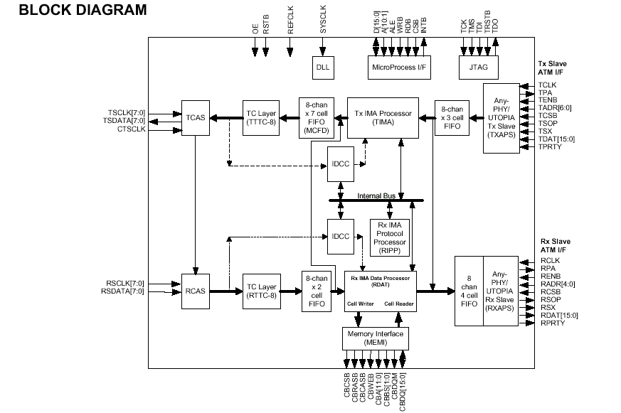
The PM7340 S/UNI-IMA-8 is a monolithic integrated circuit that implements the Inverse Multiplexing for ATM (IMA 1.1) protocol with backward compatibility to IMA 1.0 and the Transmission Convergence (TC) layer function of PM7340. IMA is a protocol designed to combine the transport bandwidth of multiple links into a single logical link. The logical link of PM7340is called a group. The S/UNI-IMA-8 PM7340 can support up to 4 independent groups with each group capable of supporting from 1 to 8 links. All links within an IMA group must be at the same nominal rate, however the link rates of PM7340 within a group can be different across groups. The S/UNIIMA- 8 can be programmed on a per link basis for cell delination or IMA.
The S/UNI-IMA-8 PM7340 supports 8 T1, E1 or unchannelized links where each link is dynamically configurable to support either IMA 1.1, backward compatible IMA 1.0, ATM over T1/E1, ATM over fractional T1/E1 or ATM HEC cell delination for unchannelized links. Unchannelized links may be used to support applications such as ADSL.
The S/UNI-IMA-8 supports a clock and data interface where eight 2-pin serial clock and data interfaces are provided. Each clock and data interface can be configured to simultaneously support combinations of either T1, E1, or unchannelized links. Unchannelized links may be used to support applications such as ADSL. Additionally, for cell delineation only, ATM over fractional T1/E1 is supported by allowing individual DS0 timeslots to be configured as active or inactive.
In the transmit direction, the S/UNI-IMA-8 accepts cells from the Any- PHY/UTOPIA interface. As per the IMA specification, the cells, destined for a group, are distributed in a round-robin fashion to the links within the group, adding IMA Control Protocol (ICP) cells, filler cells, and stuff cells as needed. The ICP cells convey state information to the far end and are used to format an IMA Frame. The IMA Frame is used as a mechanism to synchronize the links at the far end. Cell rate decoupling is performed at the IMA sub-layer via filler cells. Filler cells are used instead of physical layer cells for cell rate decoupling, thus a continuous stream of cells is sent to the TC layer. The stuff cells are used to maintain synchronization between links in a group by absorbing the rate differential that exists when links are running at slightly different rates.
The data from the IMA sub-layer is passed on to the TC layer. In the TC layer, the HEC is calculated and inserted into the cell headers; optional scrambling of the

 PM7340 Data Sheet


