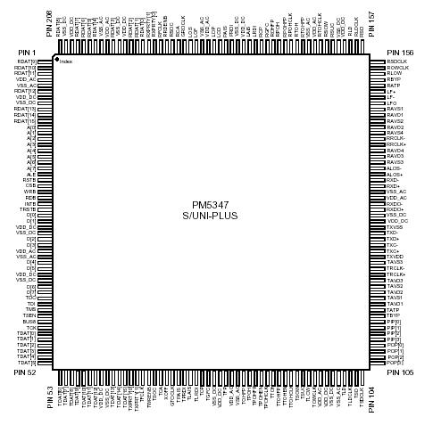
Features: · Monolithic Saturn User Network Interface that implements the ATM physical layer for Broadband ISDN according to ANSI, ITU, and ATM Forum specifications.
· Processes duplex 155.52 Mbit/s STS-3c/STM-1 or 51.84 Mbit/s STS-1 data streams with on-chip clock and data recovery and clock synthesis.
· Provides Saturn Compliant Interface - PHYsical layer (SCI-PHY™) FIFO buffers in both transmit and receive paths with parity support.
· Provides a generic 8-bit microprocessor bus interface for configuration, control, and status monitoring.
· Provides a standard 5 signal IEEE 1149.1 JTAG test port for boundary scan board test purposes.
· Low power, +5 Volt, CMOS technology.
· 208 pin high performance plastic quad flat pack (PQFP) 28 mm x 28 mm package.
· Industrial temperature range operation (-40°C to +85°C).
The receiver section:
· Provides a serial interface at 155.52 or 51.84 Mbit/s.
· Recovers the clock and data.
· Frames to and descrambles the recovered stream.
· Filters and captures the automatic protection switch channel (K1, K2) bytes in readable registers and detects APS byte failure.
· Captures the synchronization status (S1) byte in a readable register.
· Interprets the received payload pointer (H1, H2) and extracts the STS-3c/1 (STM-1) synchronous payload envelope and path overhead.
· Extracts ATM cells from the received STS-3c/1 (STM-1) synchronous payload envelope using ATM cell delineation and provides optional ATM cell payload descrambling, header check sequence (HCS) error detection and correction, and idle/unassigned cell filtering.
· Provides a generic 16 bit or 8 bit wide datapath interface to read extracted cells from an internal four cell FIFO buffer.
· Extracts all transport overhead bytes and serializes them at 5.184 Mbit/s for optional external processing.
· Extracts the section user channel (F1) and the orderwire channels (E1, E2) and serializes them into three independent 64 kbit/s streams for optional external processing.
· Extracts the data communication channels (D1-D3, D4-D12) and serializes them at 192 kbit/s (D1-D3) and 576 kbit/s (D4-D12) for optional external processing.
· Extracts all path overhead bytes and serializes them at 576 kbit/s for optional external processing.
· Extracts the 16 or 64 byte section trace (J0) sequence and the 16 or 64 byte path trace (J1) sequence into internal register banks.
· Detects loss of signal (LOS), out of frame (OOF), loss of frame (LOF), line alarm indication signal (LAIS), line remote defect indication (LRDI), loss of pointer (LOP), path alarm indication signal (PAIS), path remote defect indication signal (PRDI) and loss of cell delineation (LCD).
· Counts received section BIP-8 (B1) errors, received line BIP-24/8 (B2) errors, line far end block errors (M0 or M1), received path BIP-8 (B3) errors and path far end block errors (G1) for performance monitoring purposes.
· Counts received cells written into the receive FIFO, received HCS errored cells that are discarded, and received HCS errored cells that are corrected and passed through the receive FIFO.
· Extracts and serializes the GFC field from all received cells (including idle/unassigned cells) for external processing.
The transmitter section:
· Provides an internal four cell FIFO into which cells are written using a generic 16-bit or 8-bit wide datapath interface.
· Inserts the generic flow control (GFC) bits via a simple serial interface and provides a transmit XOFF function to allow for local flow control.
· Counts transmit cells read from the transmit FIFO.
· Provides idle/unassigned cell insertion, HCS generation/insertion, and ATM cell payload scrambling.
· Inserts ATM cells into the transmitted STS-3c/1 (STM-1) synchronous payload envelope.
· Inserts a register programmable path signal label (C2).
· Generates the transmit payload pointer (H1, H2) and inserts the path overhead.
· Optionally inserts the 16 or 64 byte section trace (J0) sequence and the 16 or 64 byte path trace (J1) sequence from internal register banks.
· Optionally inserts externally generated path overhead bytes received via a 576 kbit/s serial interface.
· Optionally inserts externally generated data communication channels (D1-D3, D4-D12) via a 192 kbit/s (D1-D3) serial stream and a 576 kbit/s (D4-D12) serial stream.
· Optionally inserts externally generated section user channel (F1) and externally generated orderwire channels (E1, E2) via three 64 kbit/s serial interfaces.
· Optionally inserts externally generated transport overhead bytes received via a 5.184 Mbit/s serial interface.
· Scrambles the transmitted STS-3c/1 (STM-1) stream and inserts the framing bytes (A1, A2).
· Synthesizes the 155.52 MHz or 51.84 MHz transmit clock from a 19.44 MHz or 6.48 MHz reference.
· Provides a serial interface at 155.52 Mbit/s or 51.84 Mbit/s.
· Optionally inserts path alarm indication signal (PAIS), path remote defect indication (PRDI), line alarm indication signal (LAIS) and line remote defect indication (LRDI) indication.
· Optionally inserts register programmable APS (K1, K2) and synchronization status (S1) bytes.
· Inserts path BIP-8 codes (B3), path far end block error (G1) indications, line BIP-24/8 codes (B2), line far end block error (M0 or M1) indications, section BIP-8 codes (B1) to allow performance monitoring at the far end.
· Allows forced insertion of all zeros data (after scrambling), the corruption of the framing bytes or the corruption of the section, line, or path BIP-8 codes for diagnostic purposes.
Application· SONET/SDH Based ATM Switching Systems
· SONET/SDH Based ATM Terminals
· B-ISDN User Network Interfaces
· B-ISDN Test EquipmentPinout Specifications
| Ambient Temperature under Bias |
-40°C to +85°C |
| Storage Temperature |
-40°C to +125°C |
| Supply Voltage |
-0.5V to +6.0V |
| Voltage on Any Pin |
-0.5V to VDD+0.5V |
| Static Discharge Voltage |
±1000 V |
| Latch-Up Current |
±100 mA |
| DC Input Current |
±20 mA |
| Lead Temperature |
+230°C |
Absolute Maximum Junction
Temperature |
+150°C |
DescriptionThe PM5347 S/UNI-PLUS SATURN User Network Interface is a monolithic integrated circuit that implements the SONET/SDH processing and ATM mapping functions of a 155 or 51 Mbit/s ATM User Network Interface.
The PM5347 S/UNI-PLUS receives SONET/SDH streams using a bit serial interface, recovers the clock and data and processes section, line, and path overhead. PM5347 performs framing (A1, A2), descrambling, detects alarm conditions, and monitors section, line, and path bit interleaved parity (B1, B2, B3), accumulating error counts at each level for performance monitoring purposes. Line and path far end block error indications (M0 or M1, G1) are also accumulated. The PM5347 S/UNI-PLUS interprets the received payload pointers (H1, H2) and extracts the synchronous payload envelope which carries the received ATM cell payload. In addition to its basic processing of the received SONET/SDH overhead, the S/UNI-PLUS provides convenient access to all overhead bytes, which are extracted and serialized on lower rate interfaces, allowing additional external processing of overhead, if desired.
The PM5347 S/UNI-PLUS frames to the ATM payload using cell delineation. HCS error correction is provided. Idle/unassigned cells may be dropped according to a programmable filter. Cells are also dropped upon detection of an uncorrectable header check sequence error. The ATM cell payloads are descrambled. The PM5347 ATM cells that are passed are written to a four cell FIFO buffer. The received cells are read from the FIFO using a generic 16- or 8-bit wide datapath interface.
Counts of received PM5347 ATM cell headers that are errored and uncorrectable and also those that are errored and correctable are accumulated independently for performance monitoring purposes.
The PM5347 S/UNI-PLUS transmits SONET/SDH streams using a bit serial interface and formats section, line, and path overhead appropriately. It synthesizes the transmit clock from a lower frequency reference and performs framing pattern insertion (A1, A2), scrambling, alarm signal insertion, and creates section, line, and path bit interleaved parity (B1, B2, B3) as required to allow performance monitoring at the far end. Line and path far end block error indications (M0 or M1, G1) are also inserted. The PM5347 S/UNI-PLUS generates the payload pointer (H1, H2) and inserts the synchronous payload envelope which carries the ATM cell payload. In addition to its basic formatting of the transmitted SONET/SDH overhead, the S/UNI-PLUS provides convenient access to all overhead bytes, which are optionally inserted from lower rate serial interfaces, allowing external sourcing of overhead, if desired. The PM5347 S/UNI-PLUS also supports the insertion of a large variety of errors into the transmit stream, such as framing pattern errors, bit interleaved parity errors, and illegal pointers, which are useful for system diagnostics and tester applications.
ATM PM5347 cells are written to an internal four cell FIFO using a generic 16- or 8-bit wide datapath interface. Idle/unassigned cells are automatically inserted when the internal FIFO contains less than one cell. The PM5347 S/UNI-PLUS provides generation of the header check sequence and scrambles the payload of the ATM cells. Each of these transmit ATM cell processing functions can be enabled or bypassed.
No line rate clocks are required directly by the PM5347 S/UNI-PLUS as it synthesizes the transmit clock and recovers the receive clock using a 19.44 MHz or 6.48 MHz reference clock. Optionally, receive clock recovery or transmit clock synthesis may be bypassed.
The PM5347 S/UNI-PLUS is configured, controlled and monitored via a generic 8-bit microprocessor bus interface. The PM5347 S/UNI-PLUS also provides a standard 5 signal IEEE 1149.1 JTAG test port for boundary scan board test purposes.
The PM5347 S/UNI-PLUS is implemented in low power, +5 Volt, CMOS technology. It has TTL and pseudo-ECL (PECL) compatible inputs and TTL/CMOS compatible outputs and is packaged in a 208 pin PQFP package.

 PM5347 Data Sheet


